Industry Plenary & Keynote
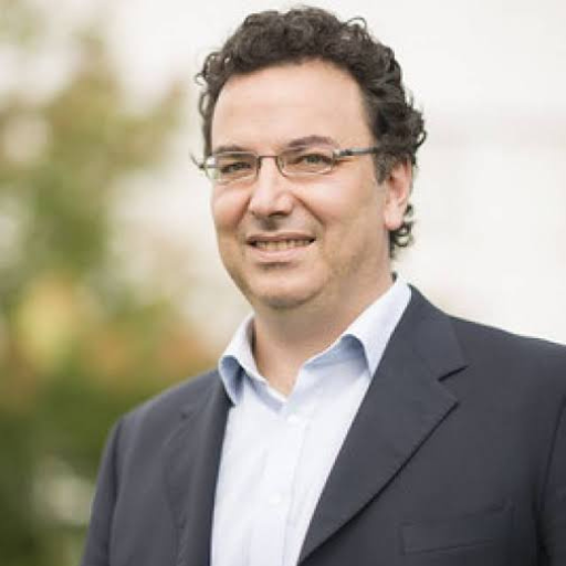
ICEE-Plenary Talk

Plenary 1: Dec 12th, 2022, Grand Ballroom, 9:30 AM - 10:30 AM

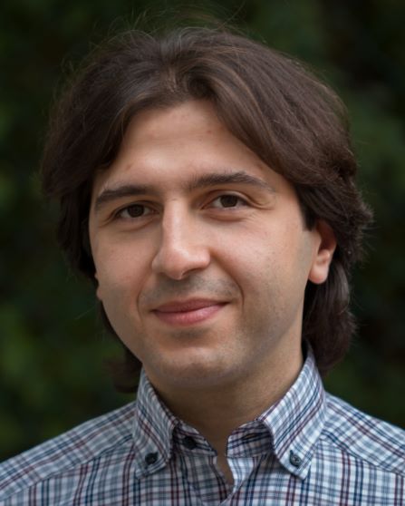
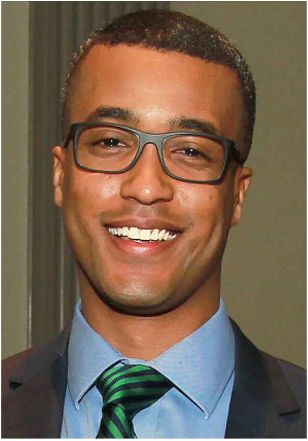
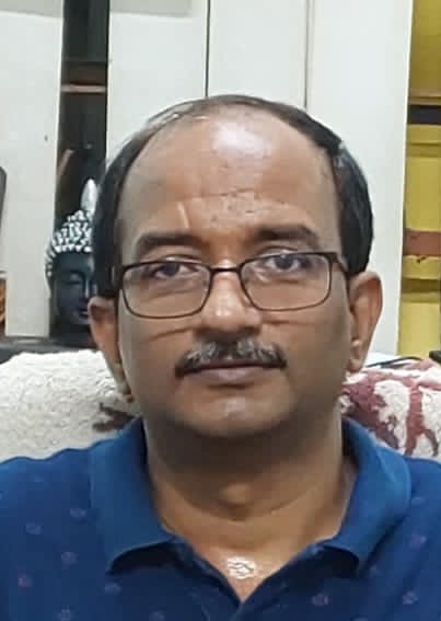
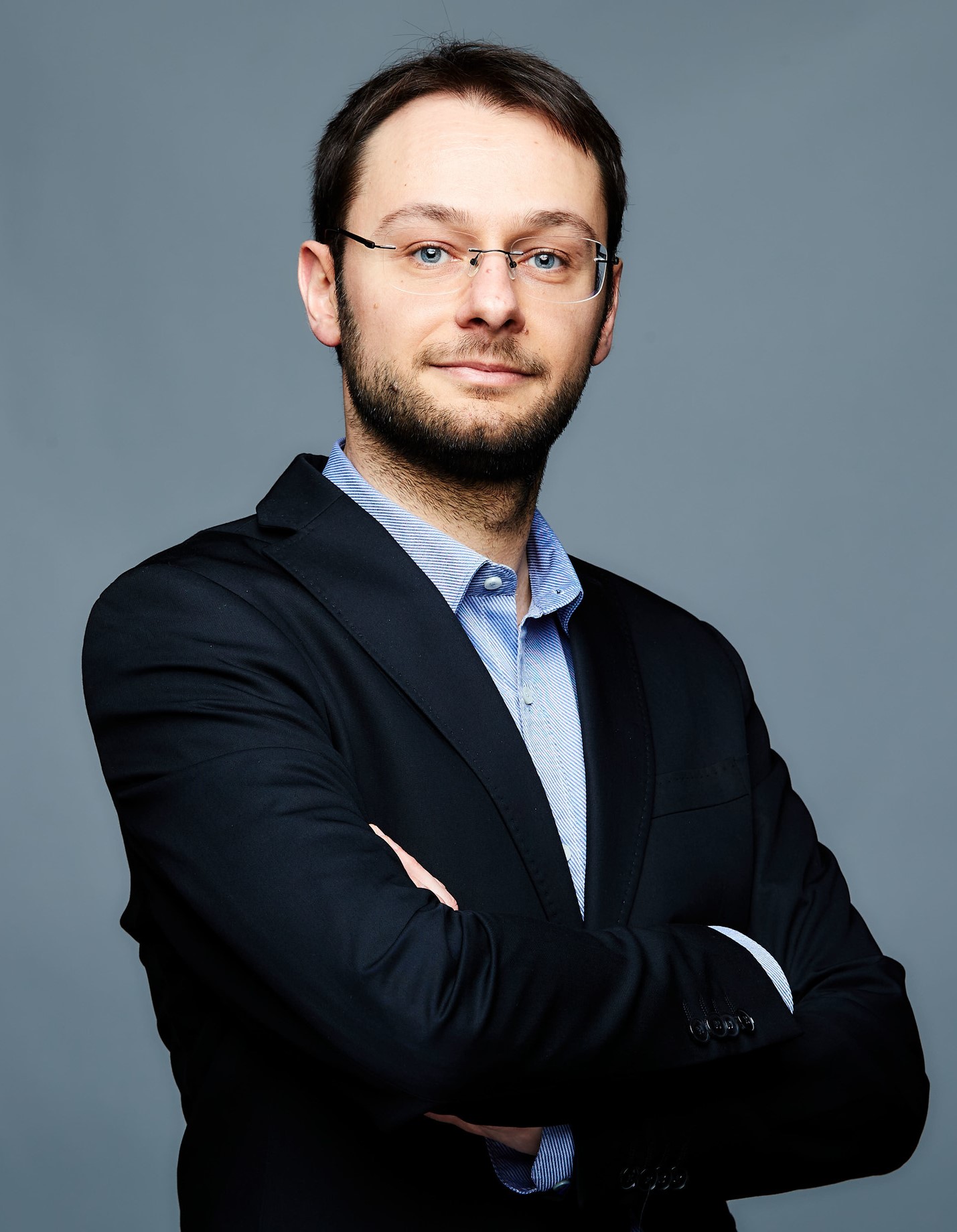
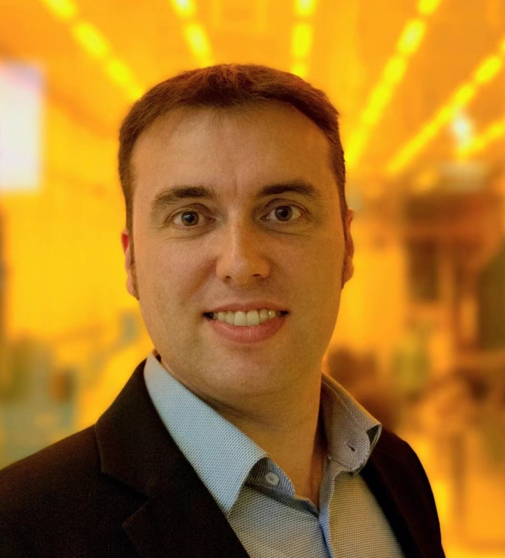
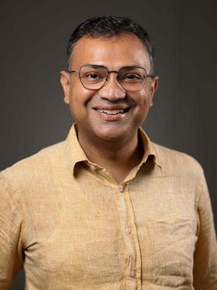
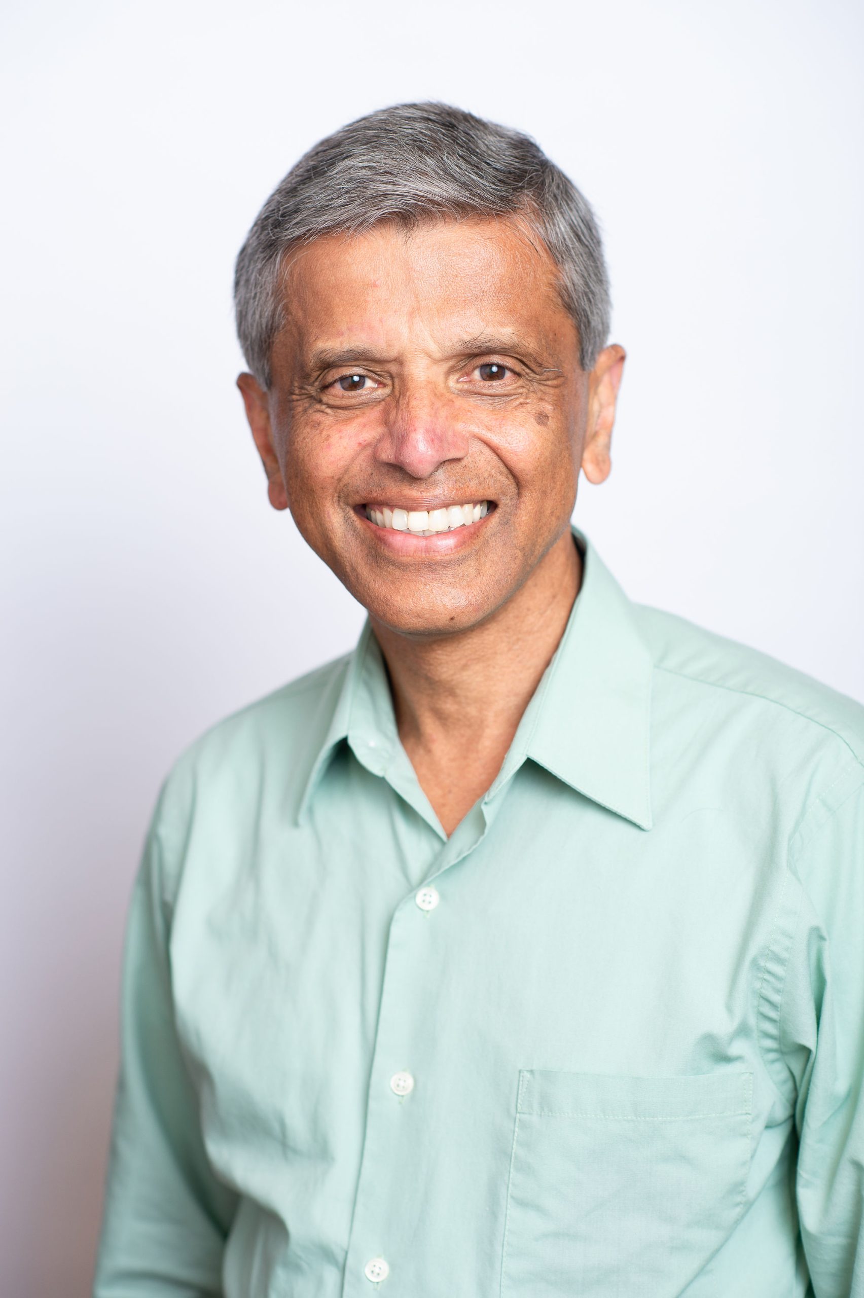
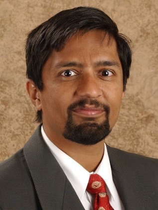
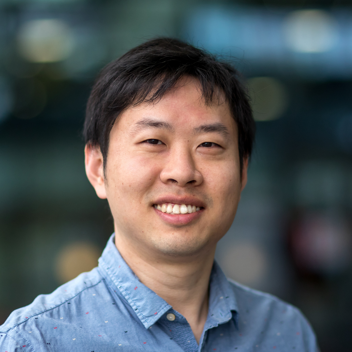
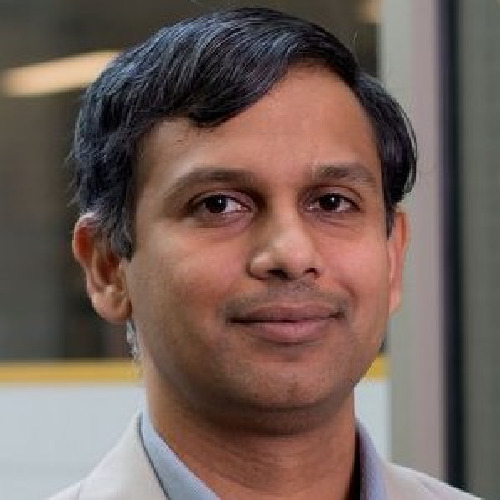
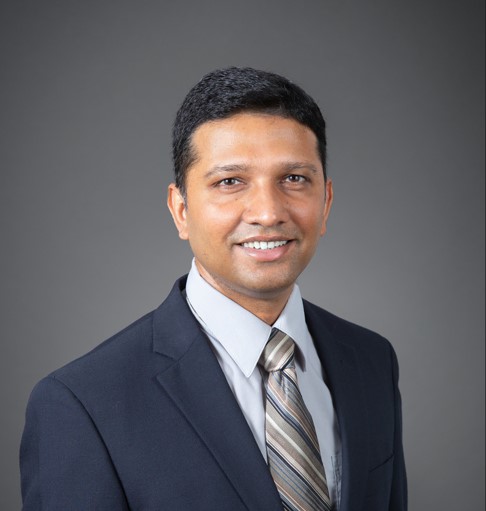
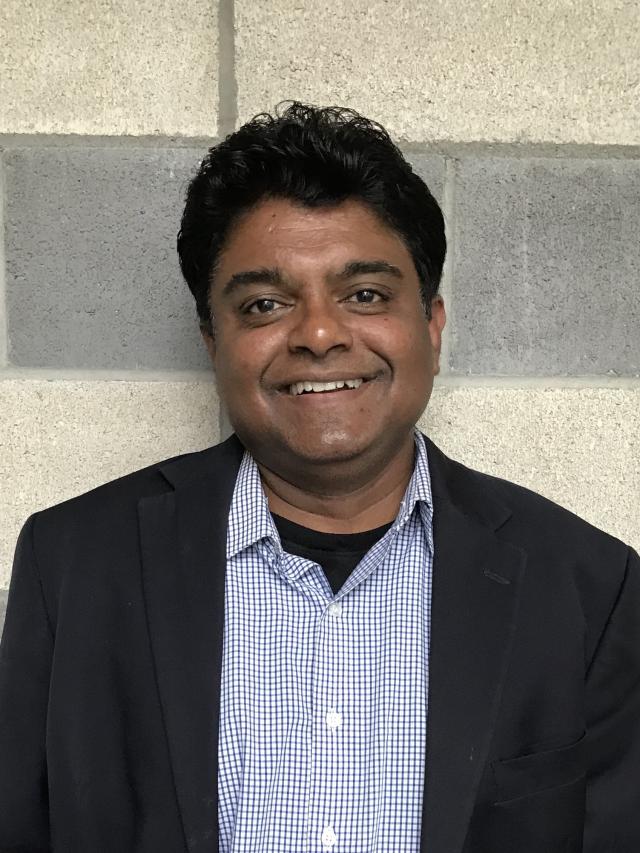
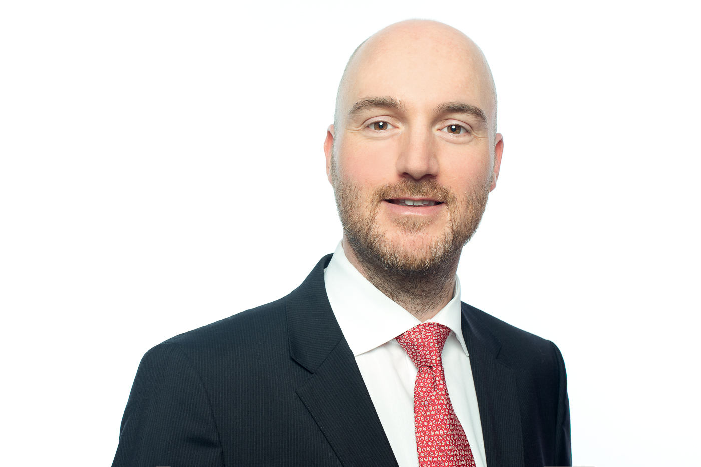
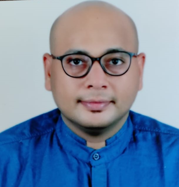
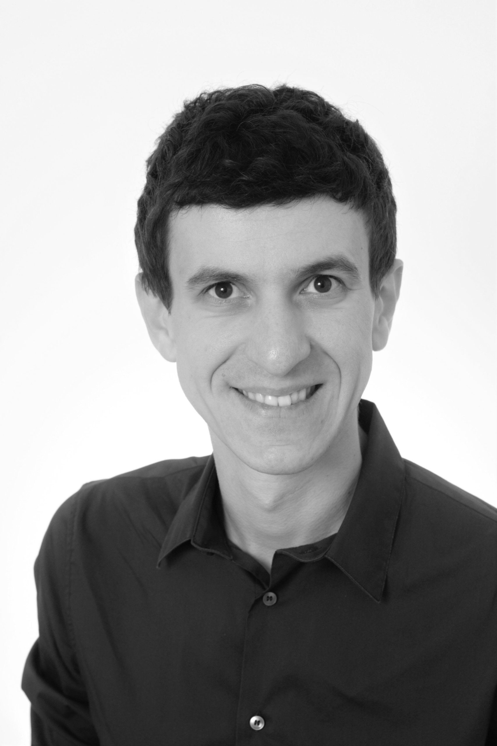
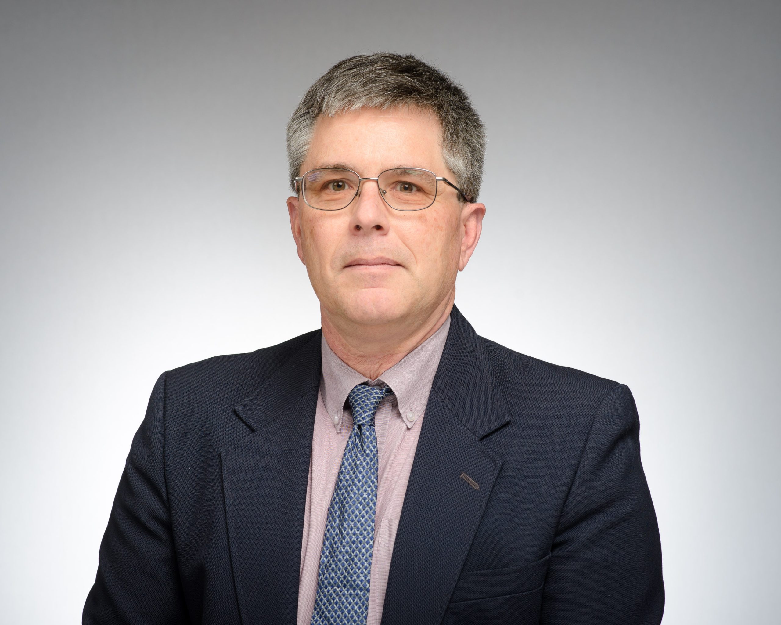
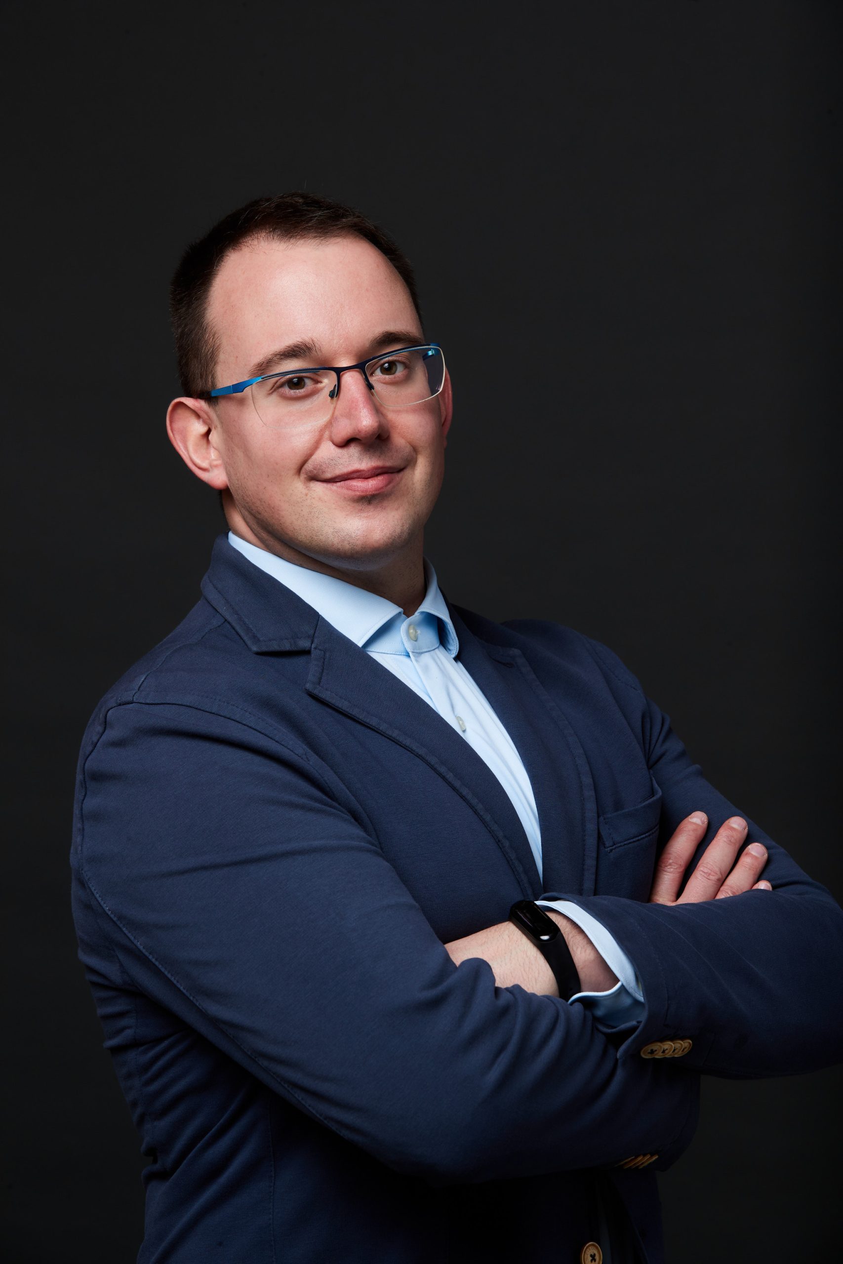
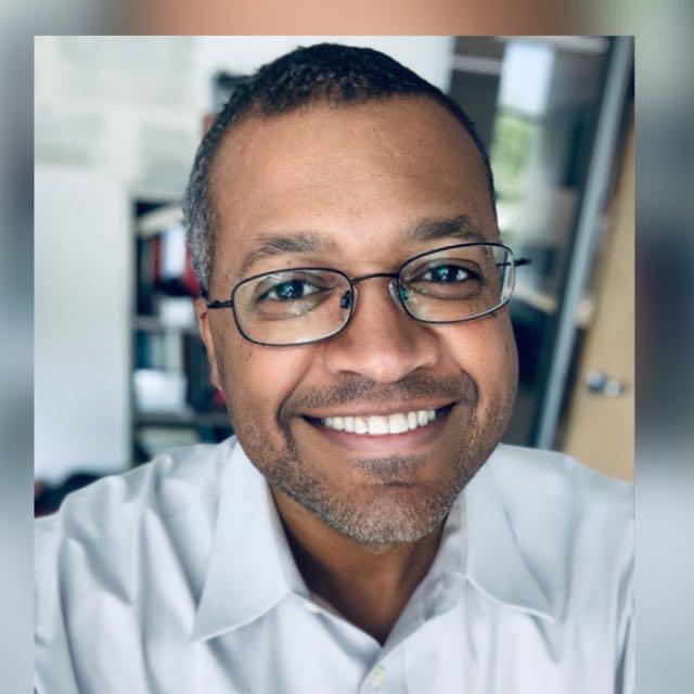
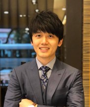
Speaker: Dr. Alessandro Curioni (IBM Fellow, Vice President, IBM, Europe & Africa and Director, IBM Research, Zurich, Switzerland)  

Title: IBM’s Quantum and Furure of Computing

Abstract: Computing is poised to reshape just about every industry, field of study — and even society itself. Across the fields of AI, cloud, and quantum computing, we’ve seen substantial advancements. The most profound advancements will be reached, though, by the convergence of classical computing, artificial intelligence and quantum, through the cloud. The result will be enormous computational power poised to fundamentally change the way we innovate and discover. In my presentation, I will discuss the latest trends, the open questions and how the academic and industrial communities may synergize to accelerate the rate of scientific discovery.

Bio: Dr. Alessandro Curioni is an IBM Fellow, Vice President of IBM Research Europe and Africa and Director of the IBM Research Lab in Zurich, Switzerland. He is responsible for IBM corporate research in Europe and leads IBM’s global research strategies in Accelerated Discovery and Security. Dr. Curioni is an internationally recognized leader in the area of high-performance computing and computational science, where his innovative thinking and seminal contributions have helped solve some of the most complex scientific and technological problems in healthcare, aerospace, consumer goods and electronics. He was a member of the winning team recognized with the prestigious Gordon Bell Prize in 2013 and 2015. Currently, his research interests include accelerating the rate of discovery with AI, Quantum, and Hybrid Cloud. Dr. Curioni received his undergraduate degree and PhD in Theoretical Chemistry from Scuola Normale Superiore, Pisa, Italy. He started at IBM Research – Zurich as a PhD student in 1993 before officially joining as a research staff member in 1998. Since then, he has had several research and manager roles, including as the founding manager of the Cognitive Computing and Computational Sciences department. He is a member of the Swiss Academy of Technical Sciences

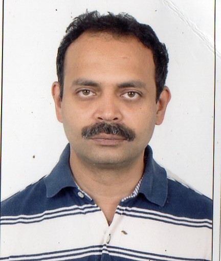
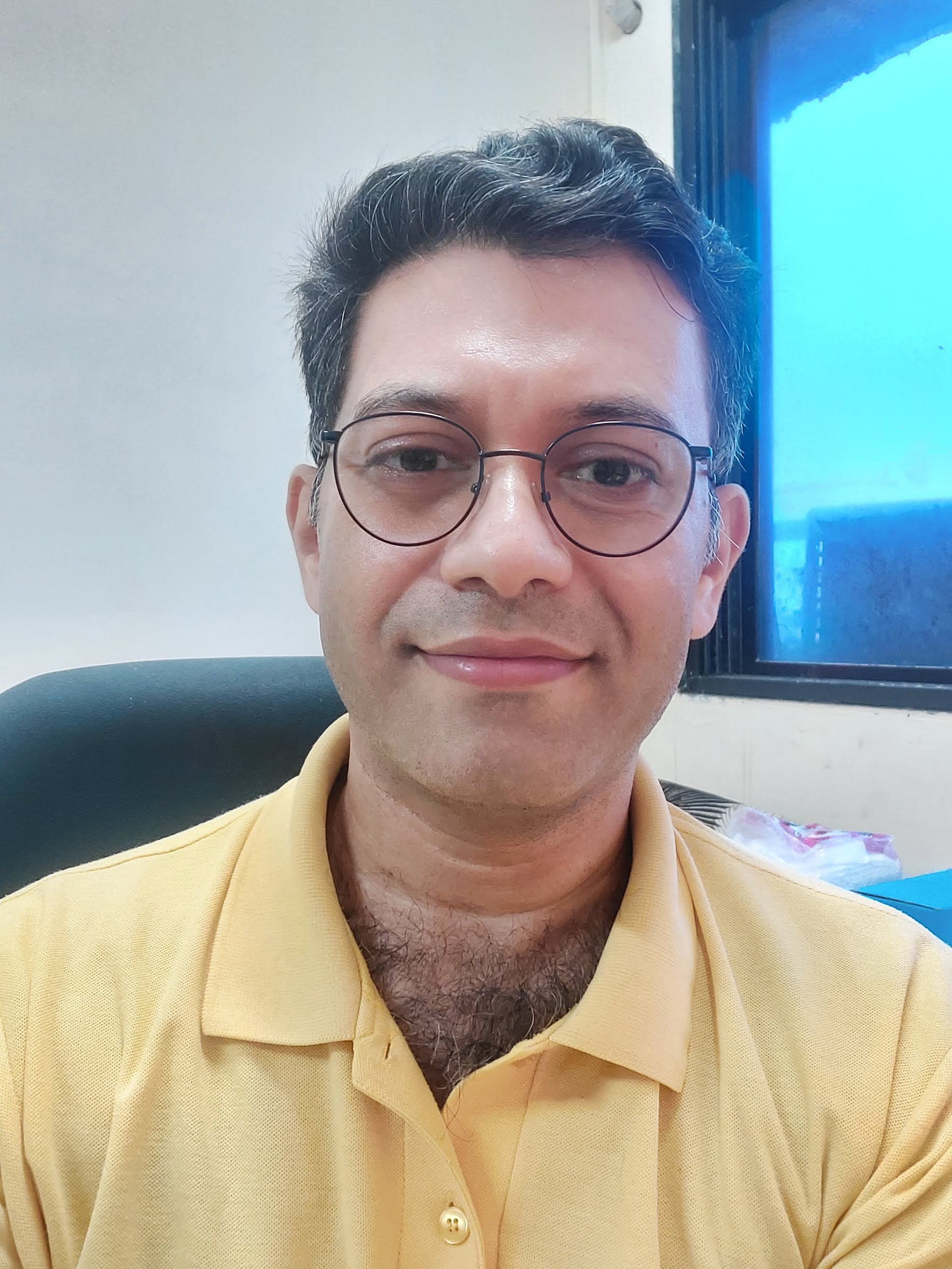
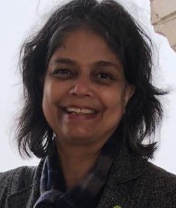
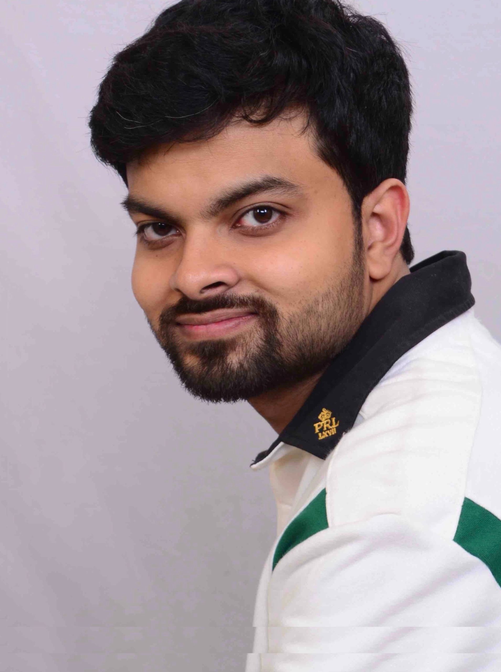
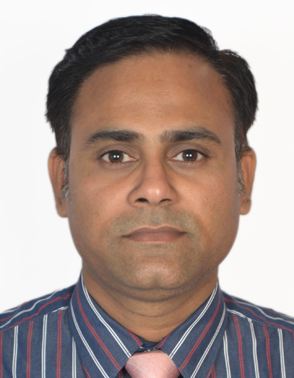
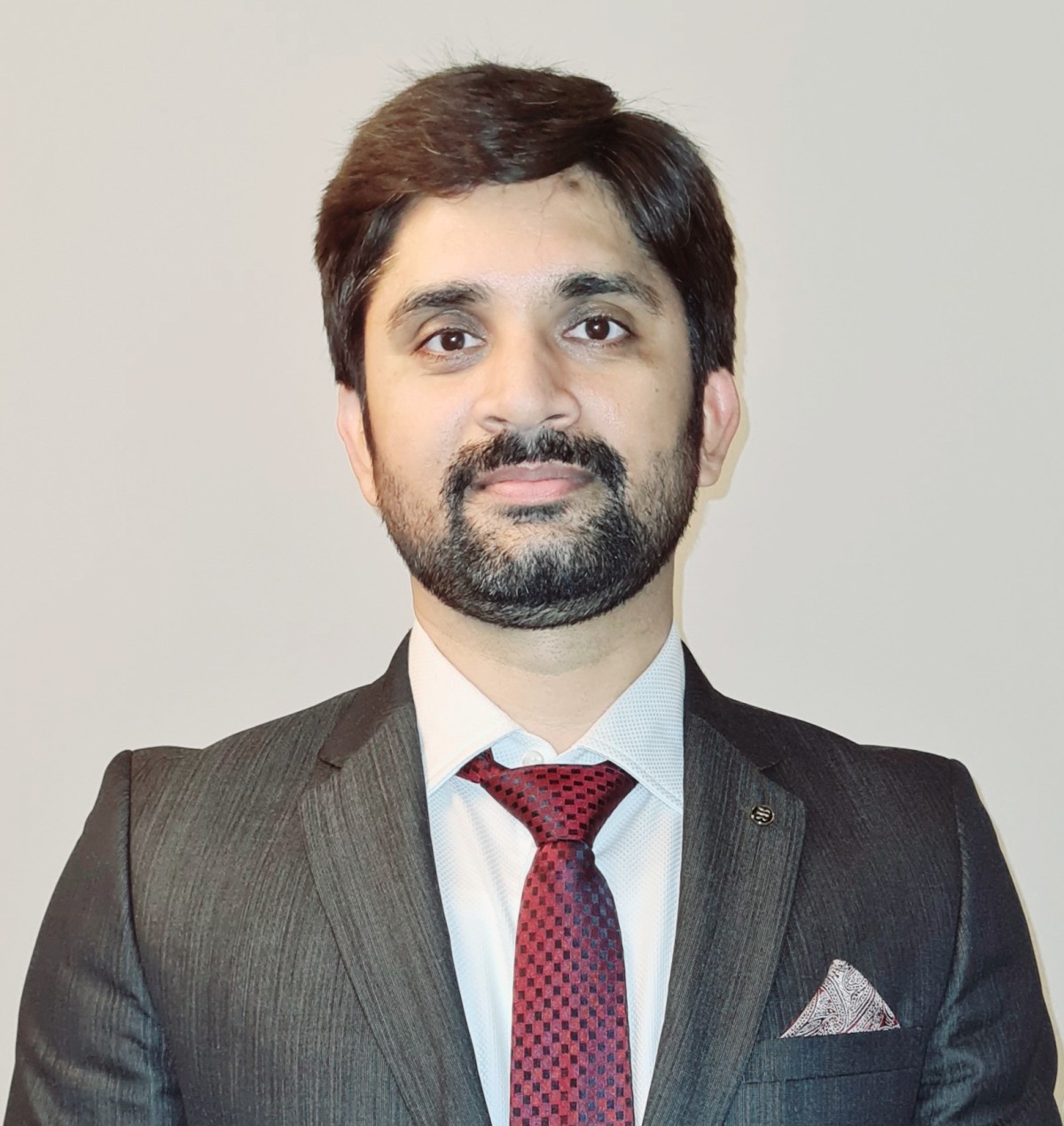
sameer

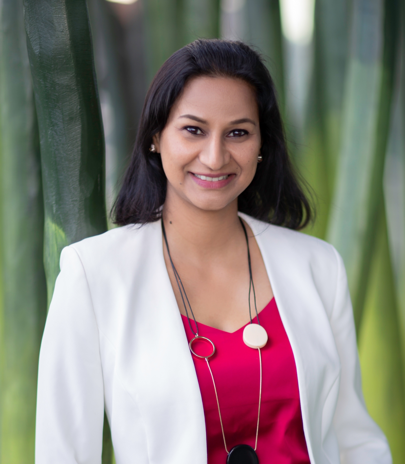
Plenary 2: Dec 13th, 2022, Grand Ballroom, 9:00 AM - 10:00 AM

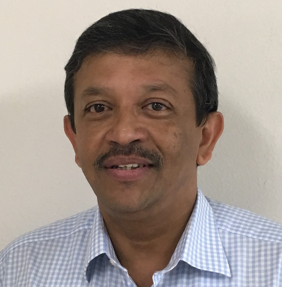
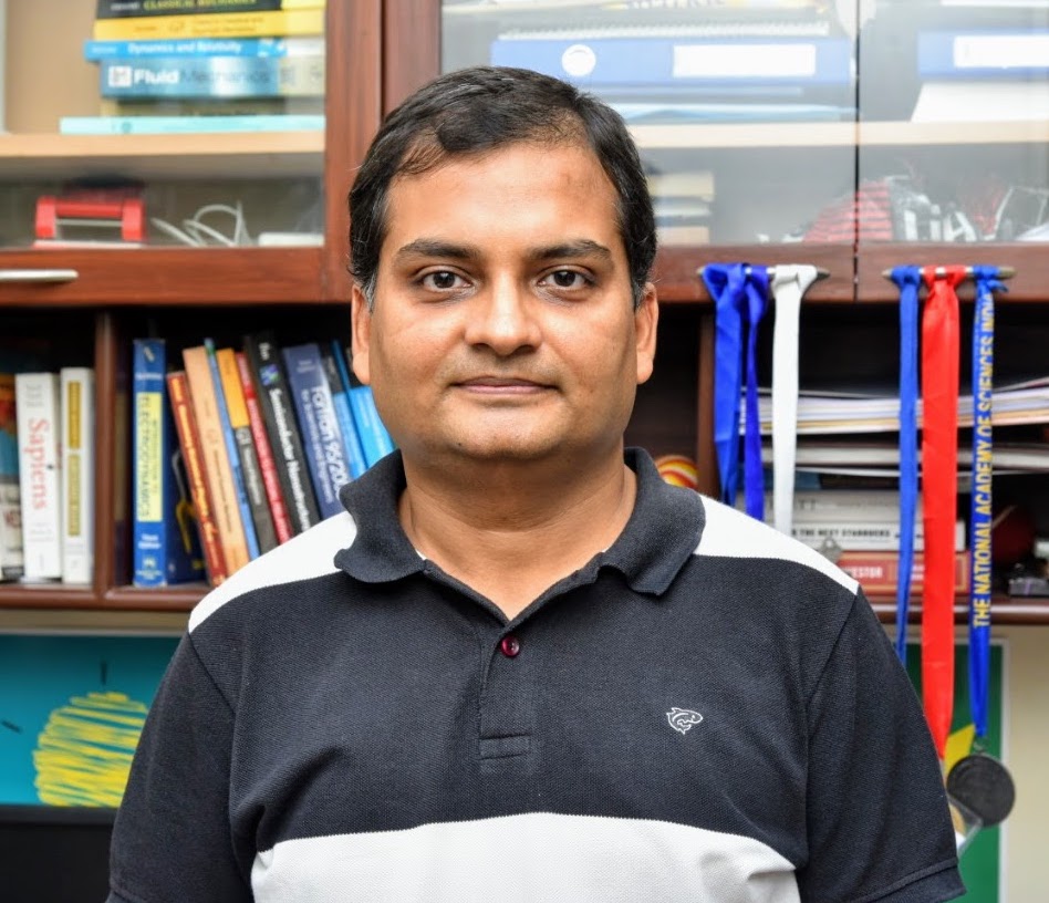
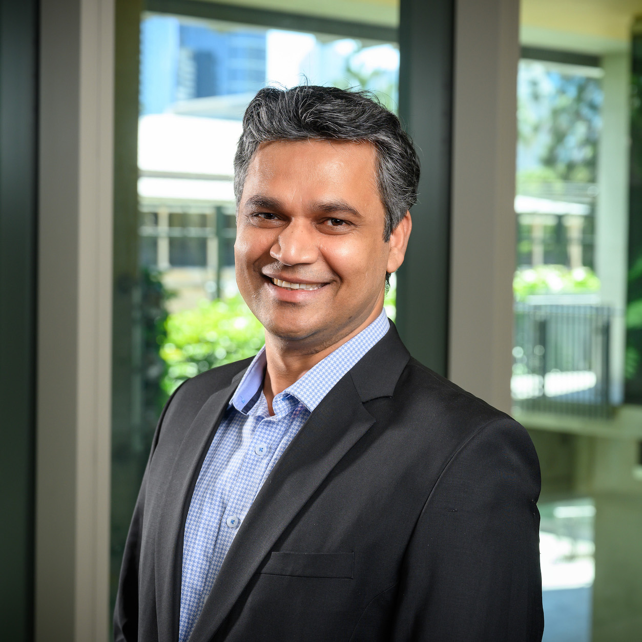
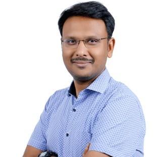
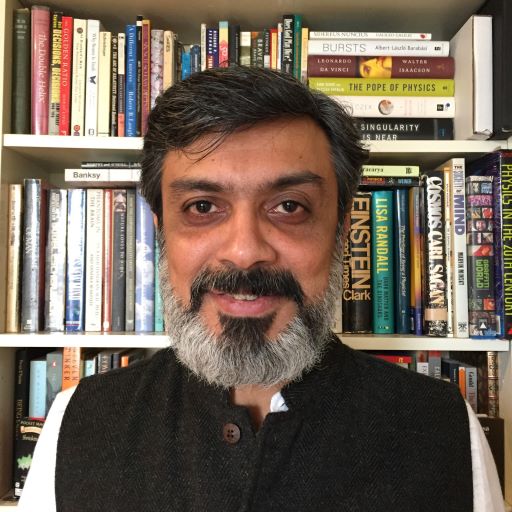
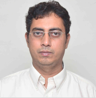
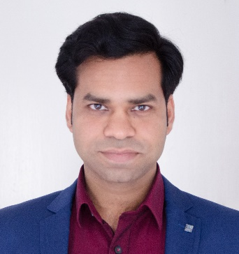
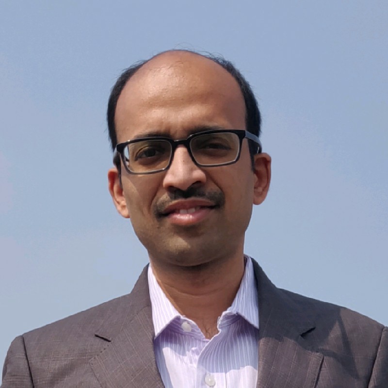
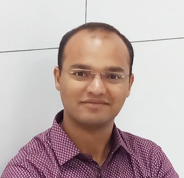
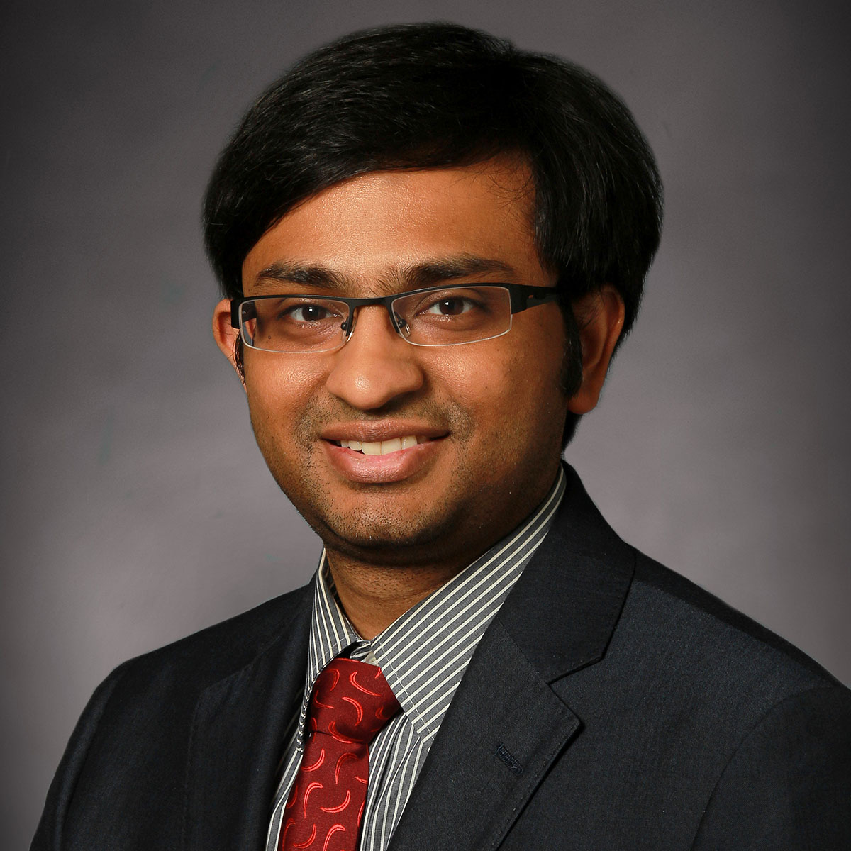
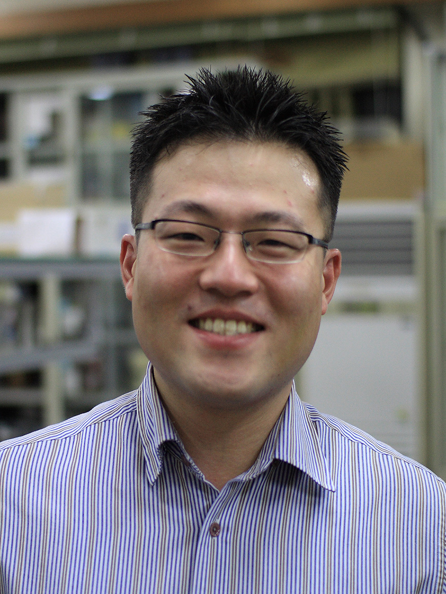
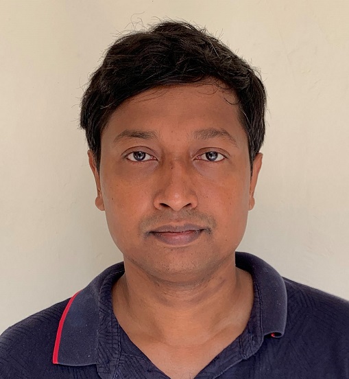
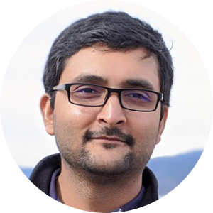
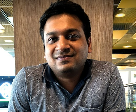
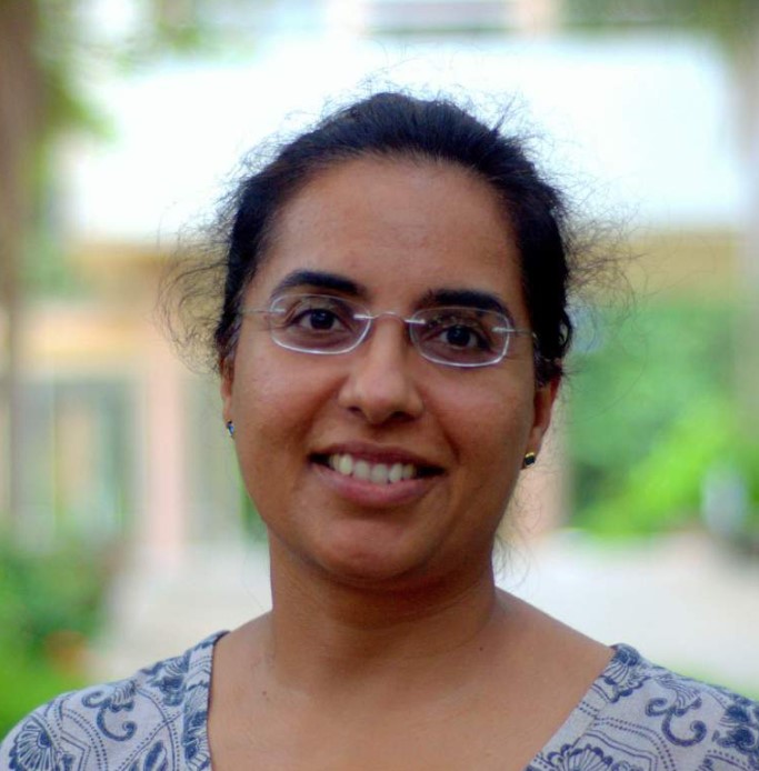
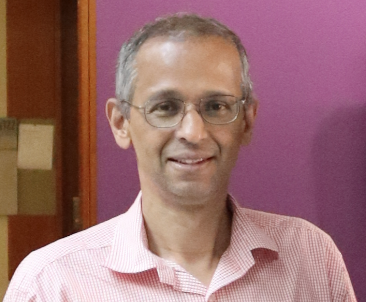
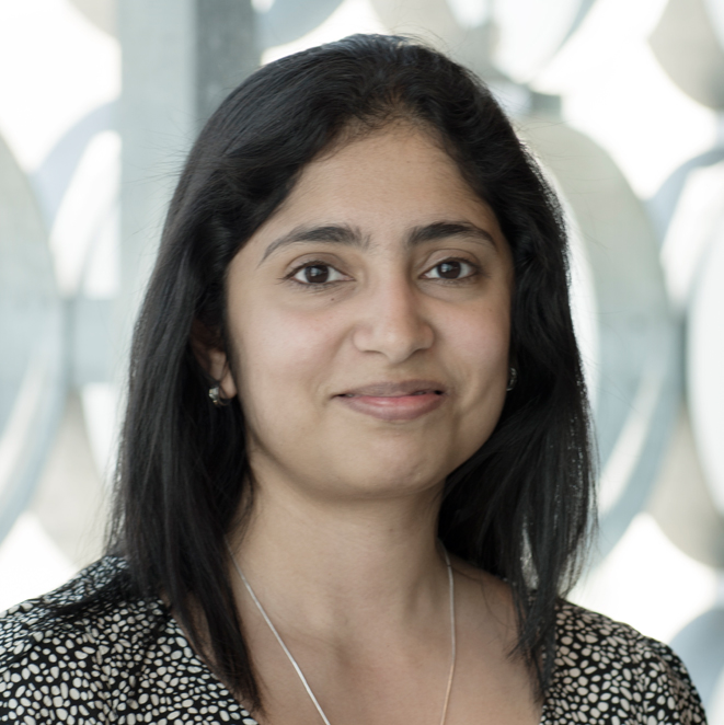
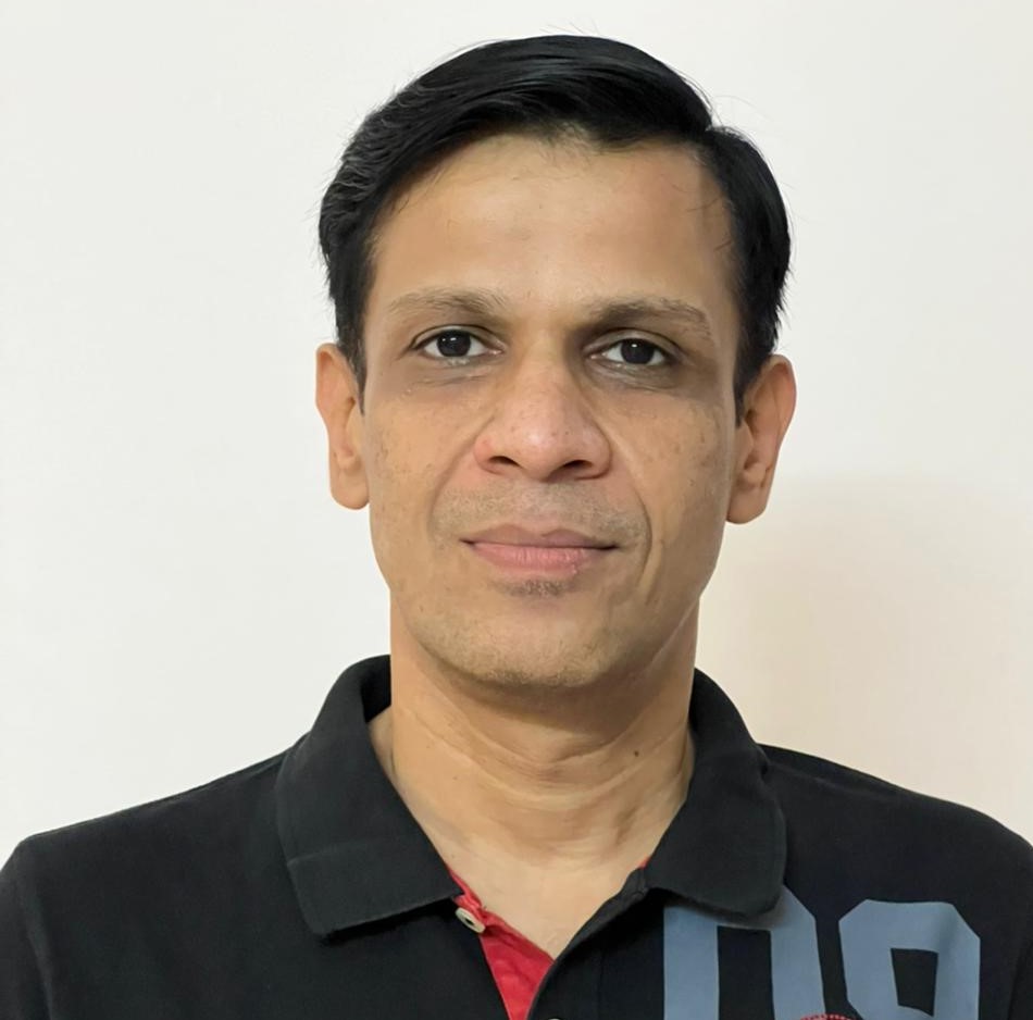
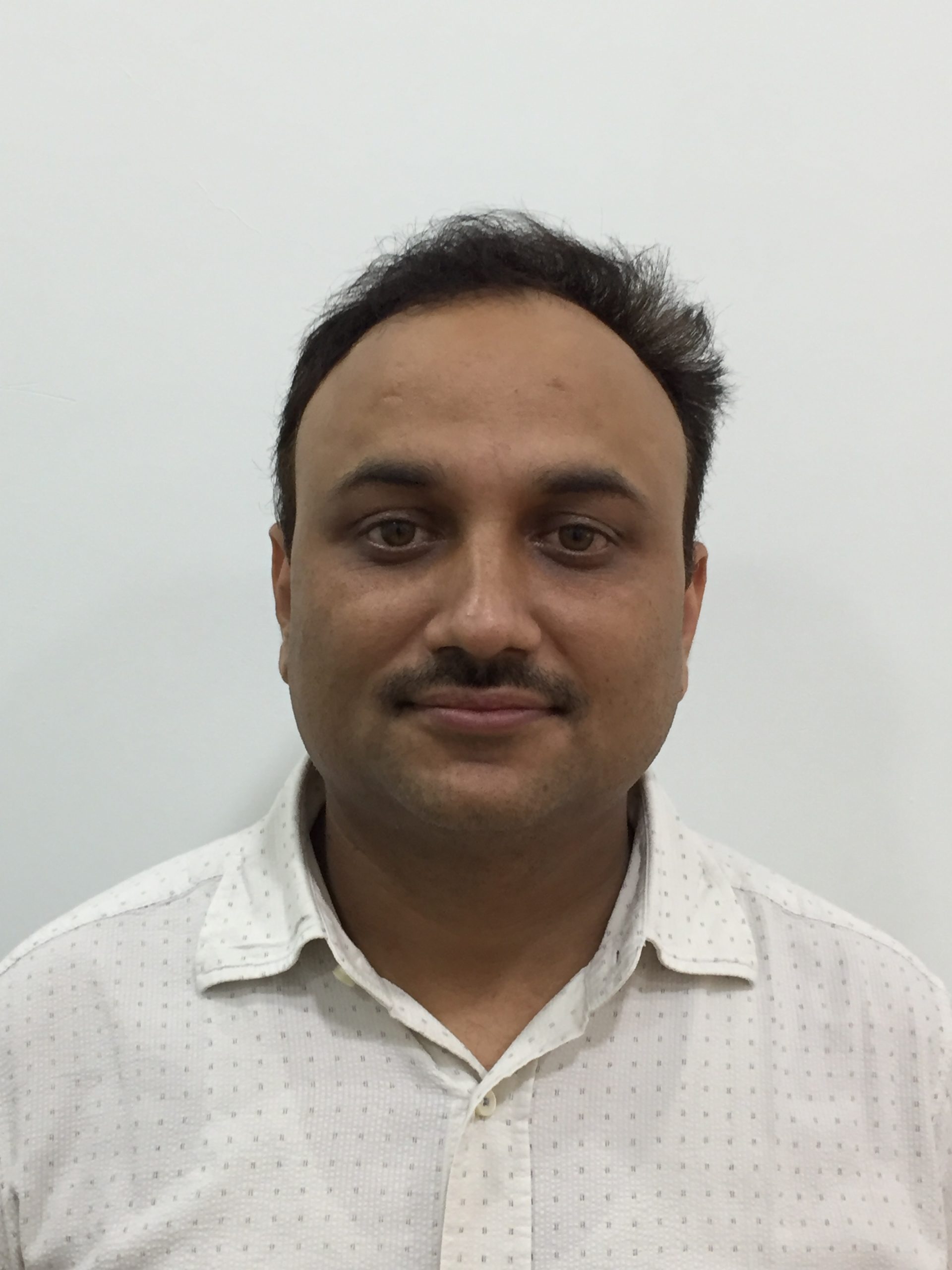
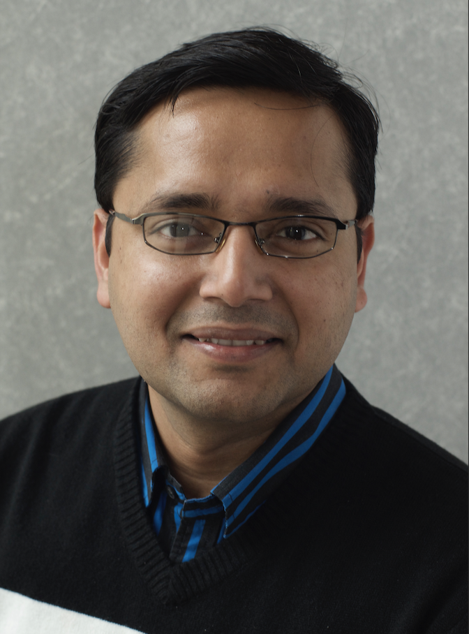
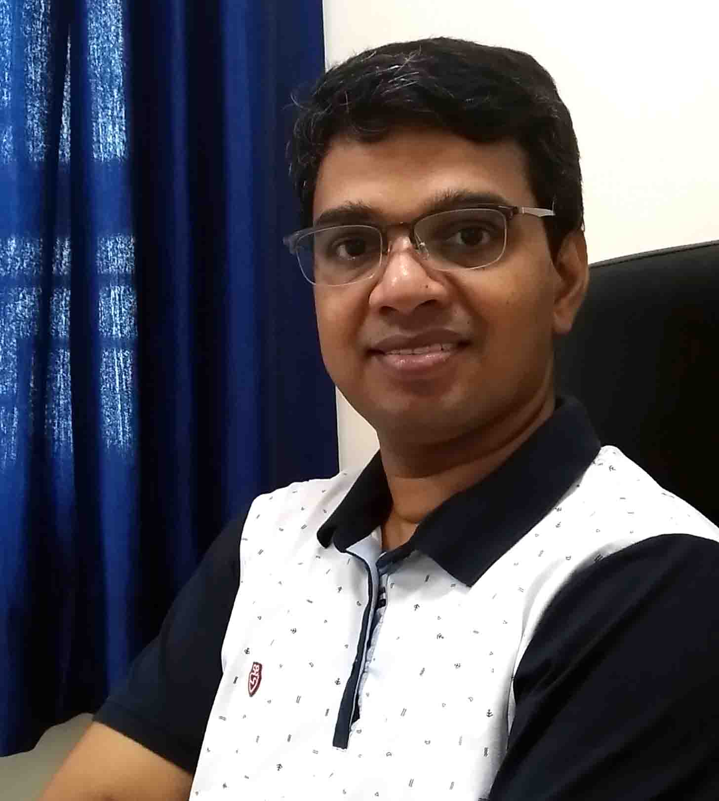
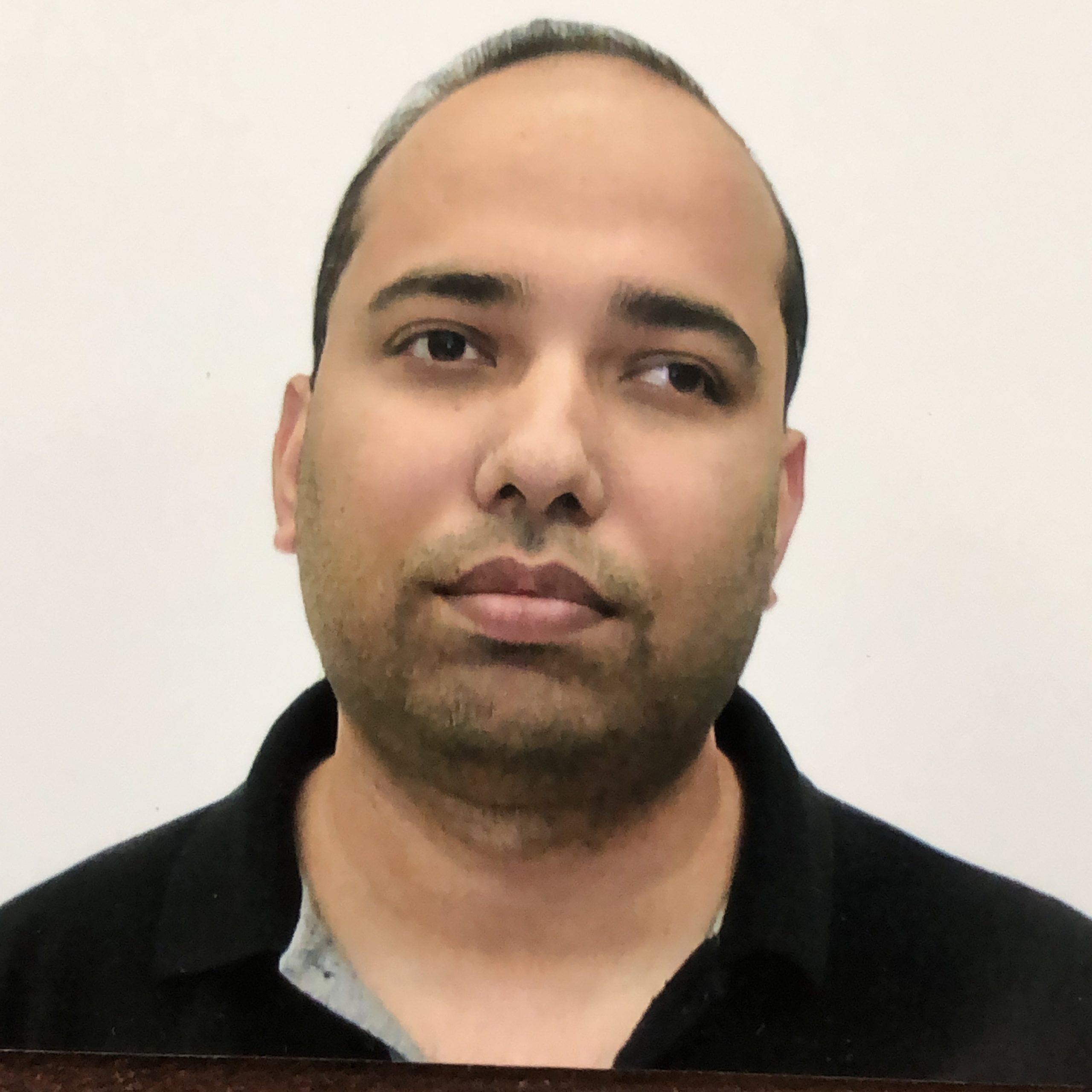
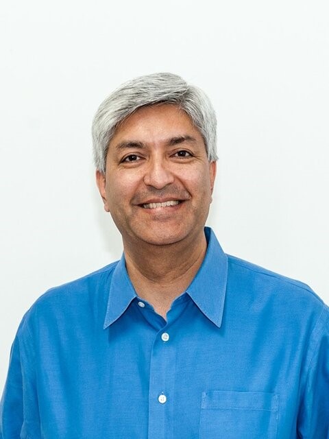
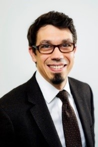
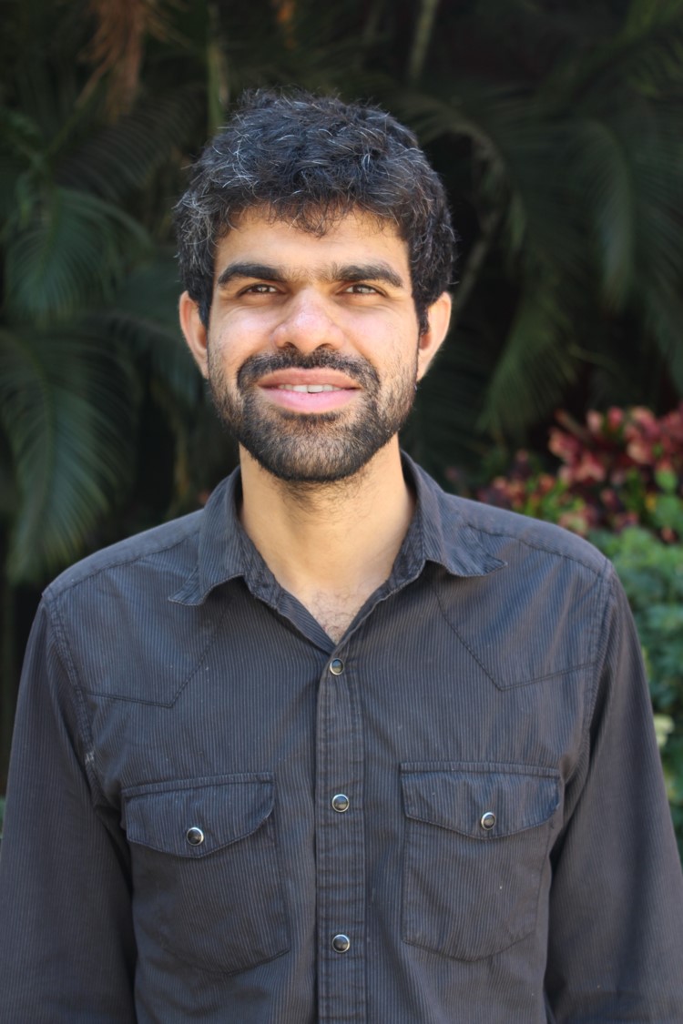
Speaker: Mr. Sameer Pendharkar (Vice President, Technology Development and TI Senior Fellow at Texas Instruments)

Title: Analog and Power Technologies for Industrial and Automotive Electronics

Abstract: With increase in per capita energy consumption and limited energy resources, it is critical to not only look at alternate energy sources but also to improve the efficiency in how this energy is used. New advances in semiconductor materials and technologies continue driving increasing electronics adoption in industrial and automotive systems making them more efficient. Innovations in multi-domain mixed signal integration are driving Industry 4.0 whereas significant improvements in power density and high voltage technology are enabling automotive electrification. The talk will focus on the trends and performance improvements in both the silicon and WBG semiconductor IC technologies targeted for these applications and also discuss the manufacturing challenges and opportunities for these technologies.

Bio:  Sameer completed his undergraduate studies and graduate studies in Electrical Engineering from the Indian Institute of Technology, Bombay and the University of Wisconsin-Madison respectively. He joined TI in 1996 and is currently a TI Senior Fellow and Vice President of Technology Development. Sameer and his team are responsible for setting and executing the overall technology development strategy for TI. He also serves on the Board of Directors of the Semiconductor Research Corporation (SRC). He has published more than 95 technical papers in leading academic journals and conferences and has been granted more than 175 U.S. patents.

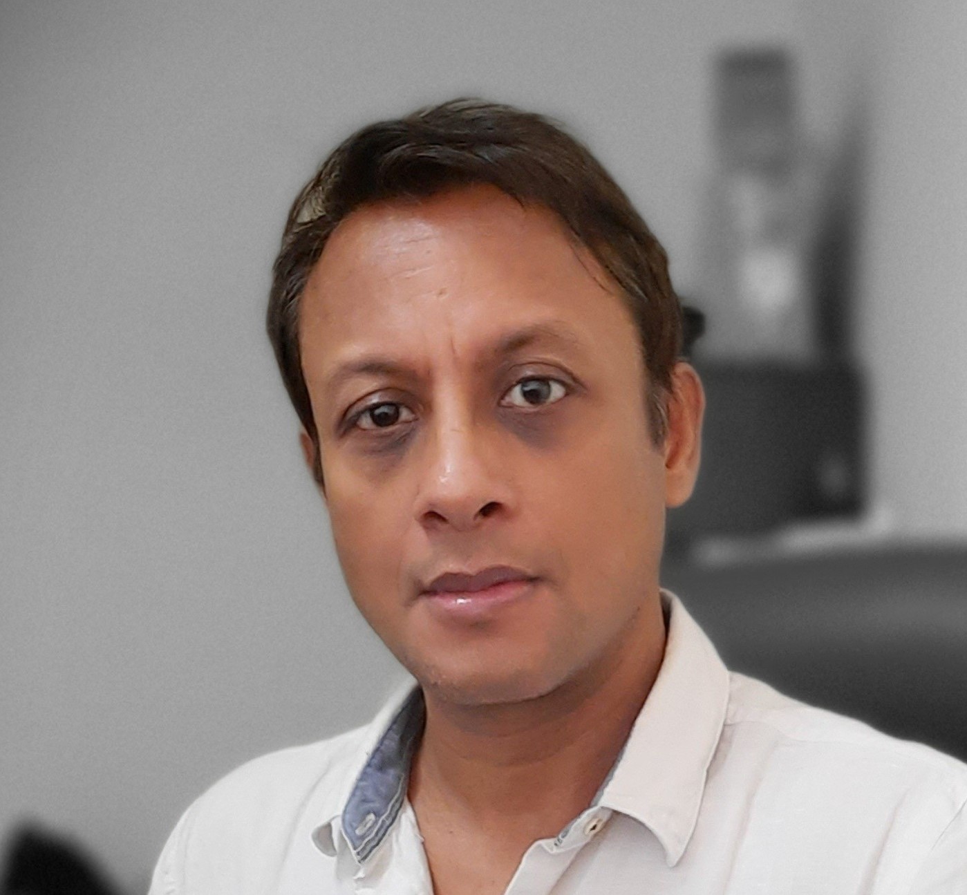
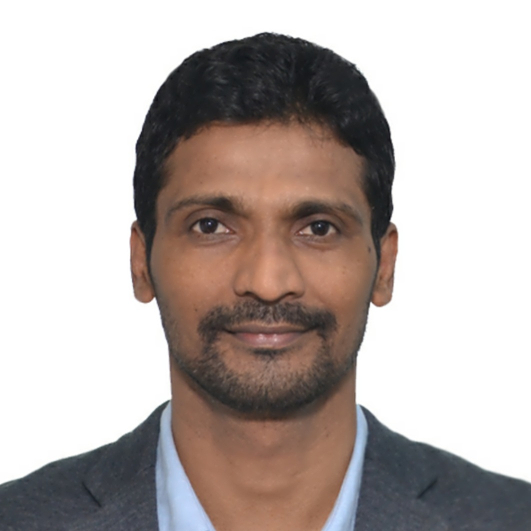
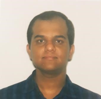
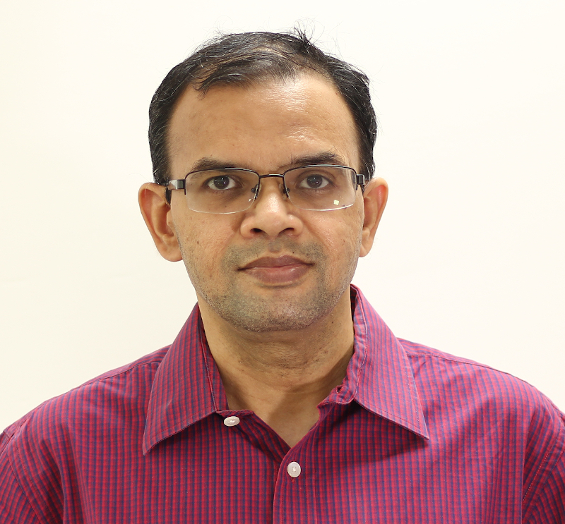
balajee

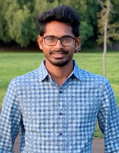
Plenary 3: Dec 14th, 2022, Grand Ballroom, 9:00 AM - 10:00 AM

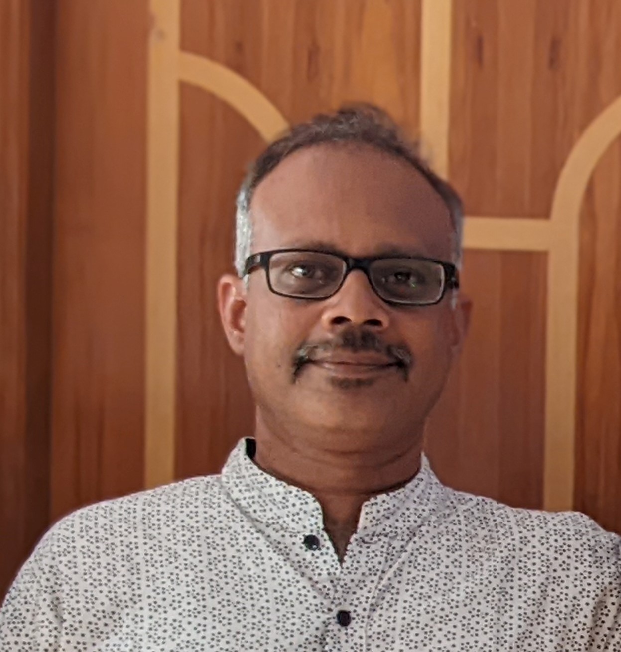
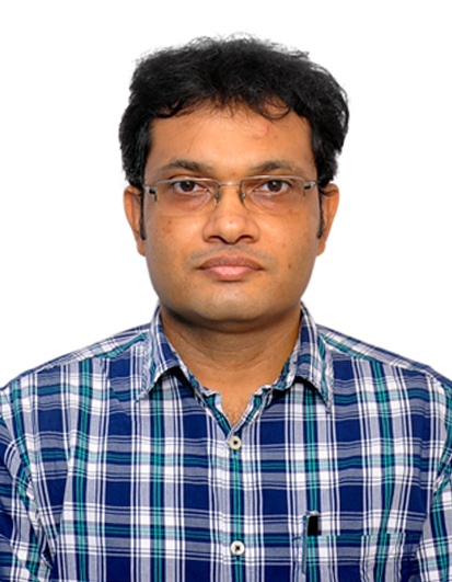
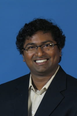
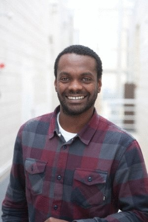
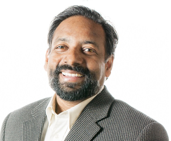
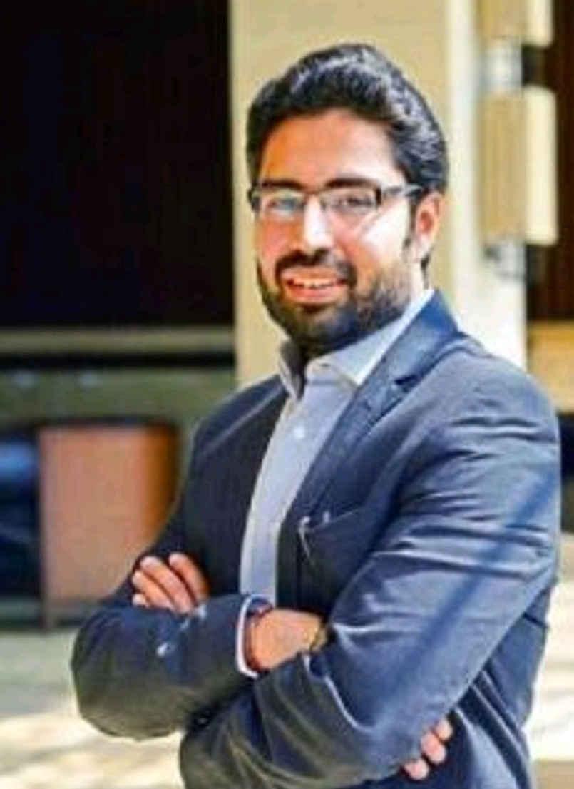
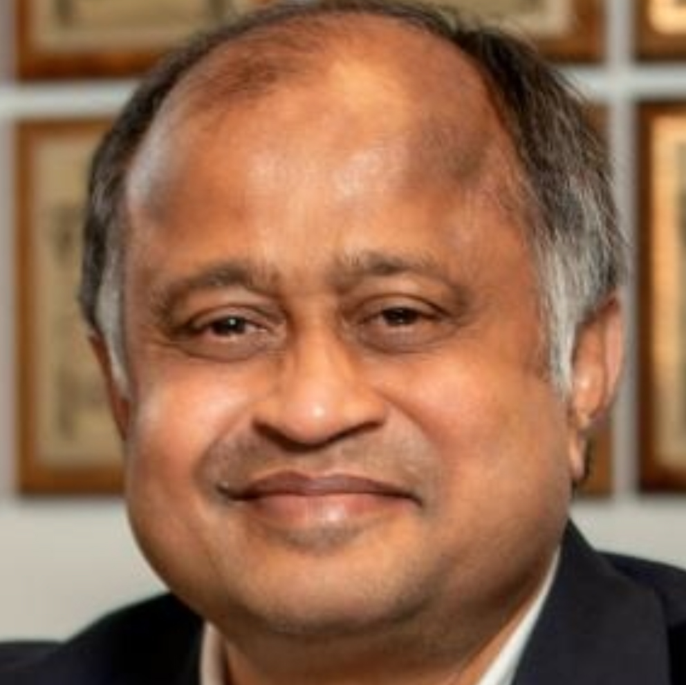
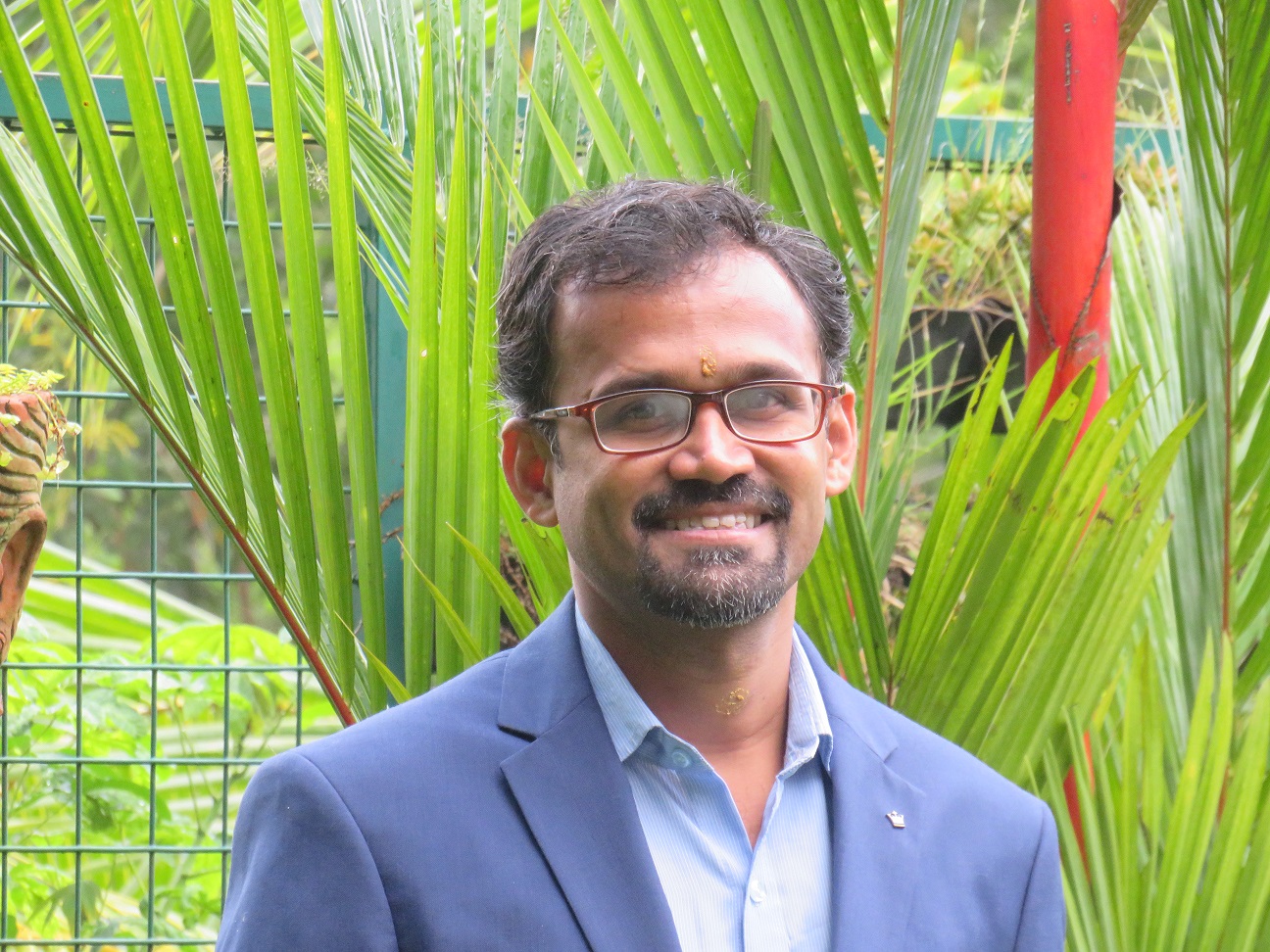
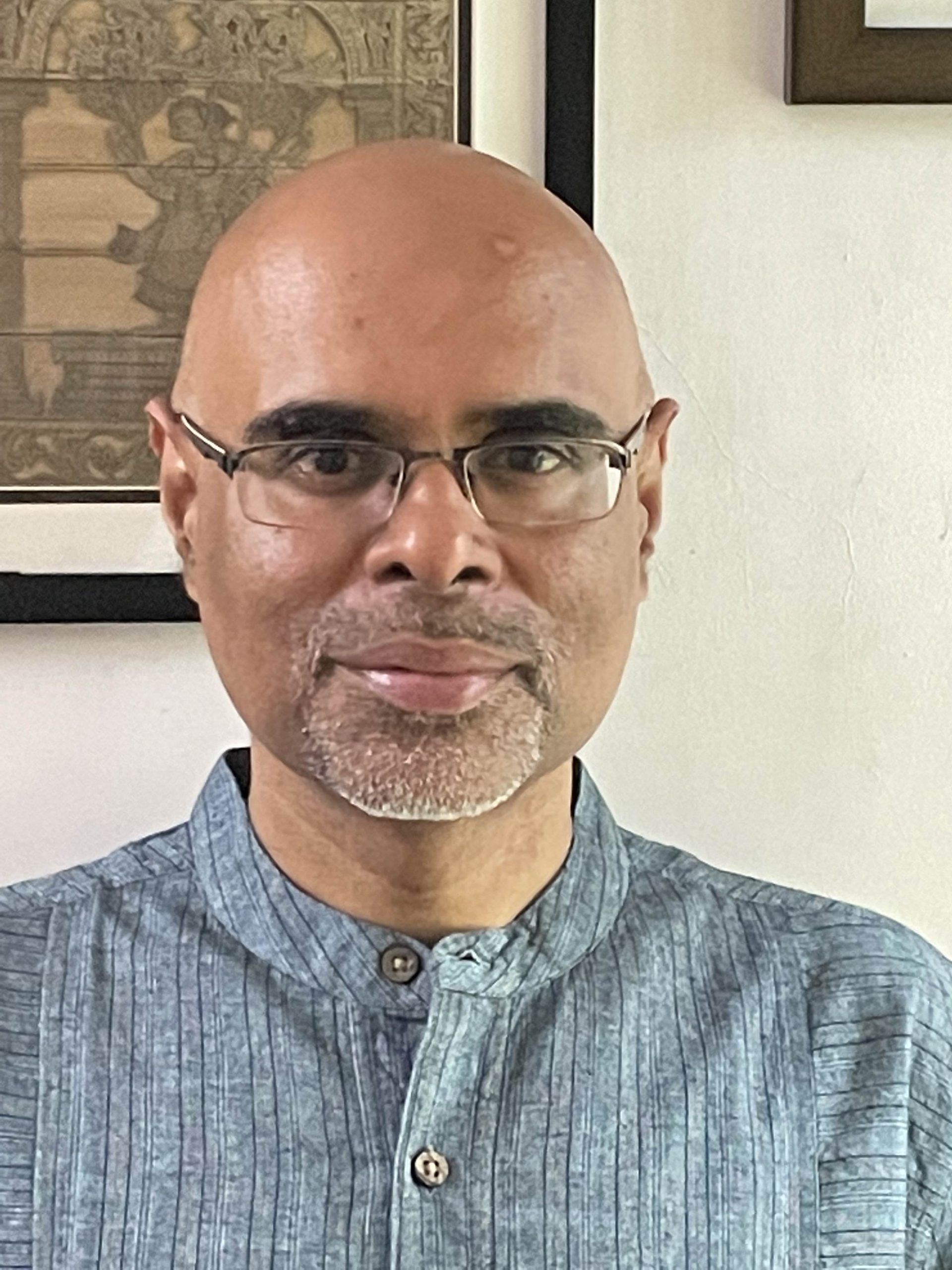
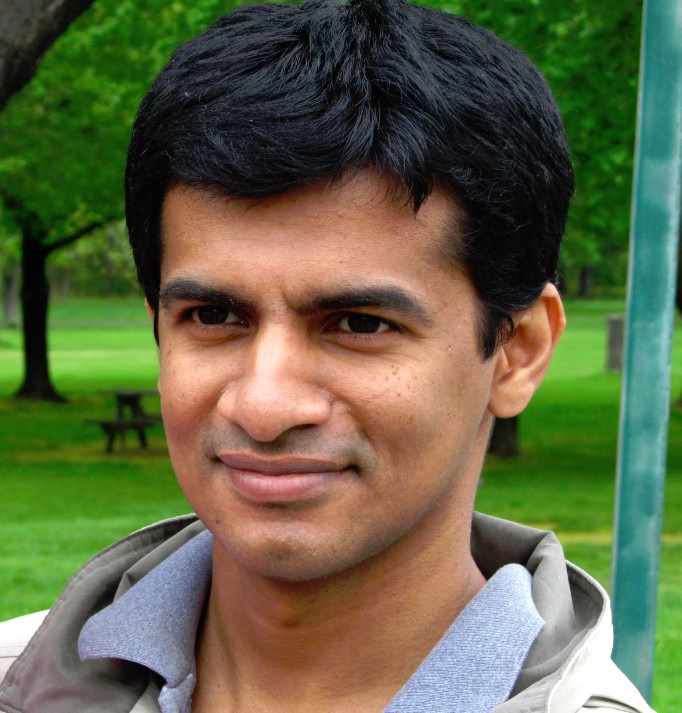
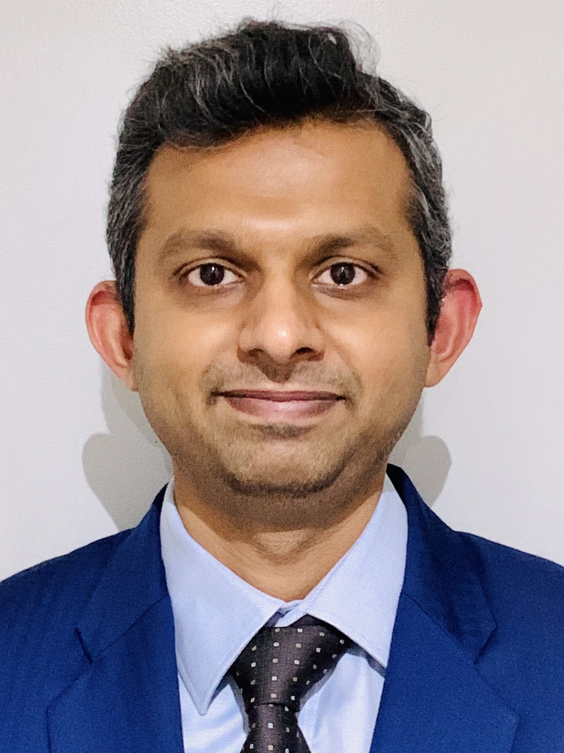
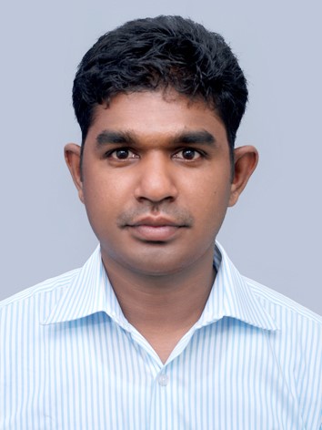
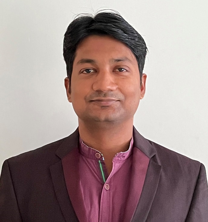
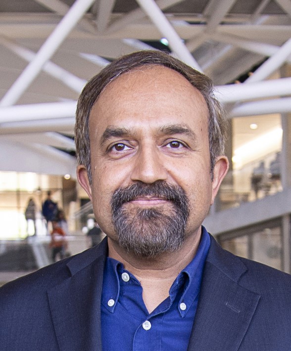
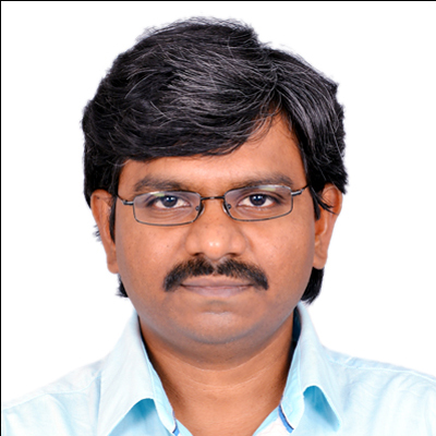
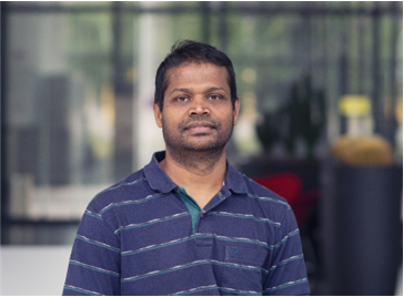
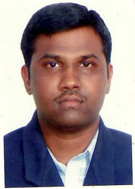
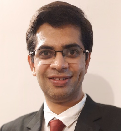
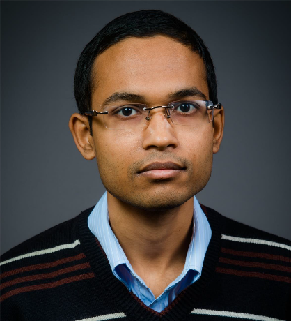
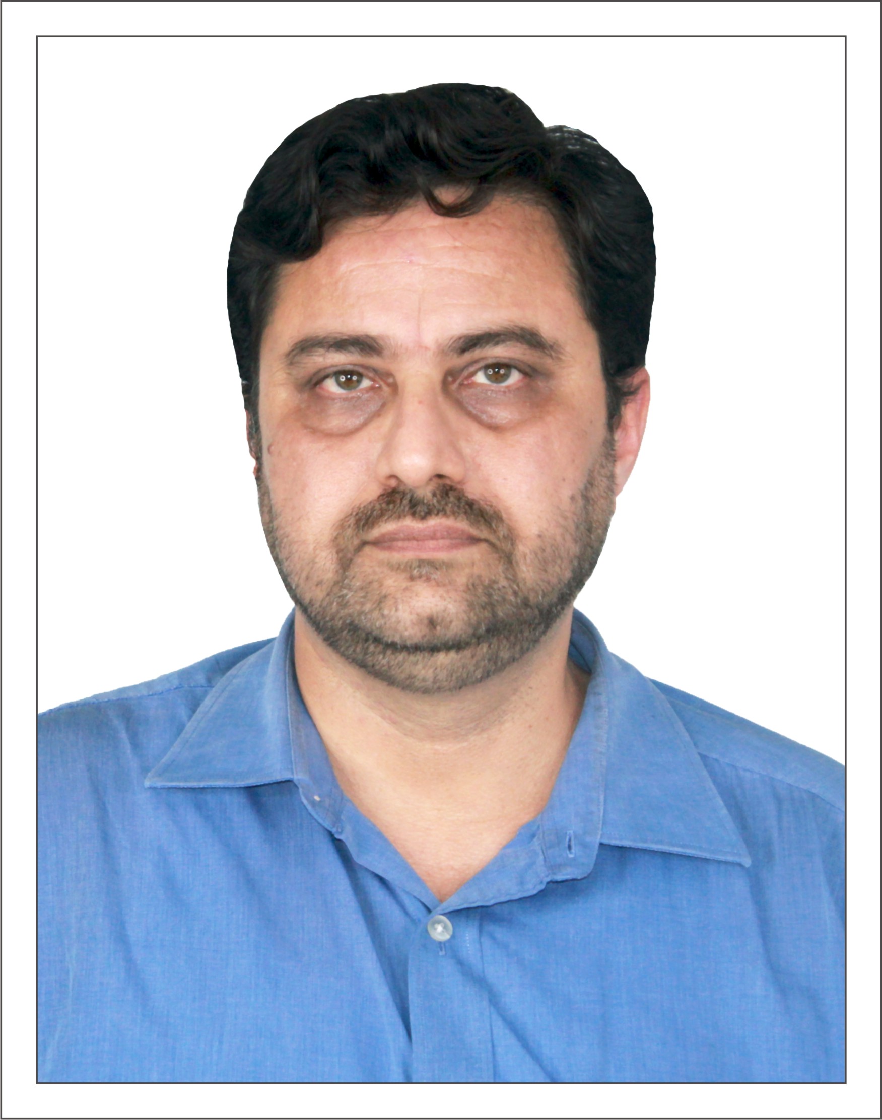
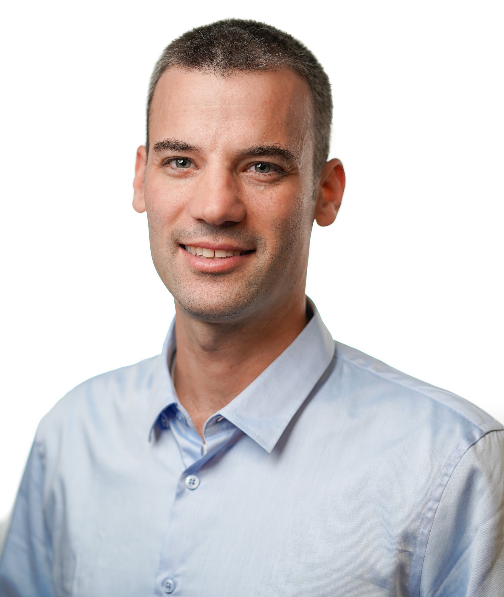
Speaker: Mr. Balajee Sowrirajan (Vice President, Samsung Electronics & MD Samsung Semiconductor R&D, India)

Title: System Solutions Powering Intelligent Connected Device

Abstract:  With Industrial Revolution 4.0 driving exciting use models, system solutions are powered by devices which are not just connected, but also Intelligent. The talk will focus on fundamental technology anchors – Connectivity, Sensors, Big Data and AI Processing solutions. It will focus on the technological advancements in these areas which are and will be transforming our day to day lives.

Bio:  Balajee Sowrirajan, is the head of Samsung Semiconductor India R&D Center (SSIR), overseeing India operations of the Memory, System LSI, Foundry business units and driving both strategy and culture for innovation and inclusion at SSIR. With a Masters degree in Engineering in Computer Science from BITS, Pilani, Balajee has played a crucial role in the journey of SSIR. With three decades of corporate experience in the Semiconductor industry, he has spent more than 9 years focusing on the expansion and building of excellence for three teams at SSIR. Samsung’s memory business continues to maintain its top market share for close to three decades. The Memory team at SSIR is an integral part of enabling embedded, client, Data Center & Enterprise Solutions for Samsung Electronics. As the Corporate VP and Head of System LSI Business, Balajee strives to bring in excellence in designs while guiding the team towards development of key components for Mobile and Automotive Electronics business such as System on Chip (SOC), Cellular Modem (4G/5G), WiFi/BT chips, power management IC, Display driver chips and CMOS image sensors. In addition, the Foundry business is also the second largest foundry supplier in the world; developing the first 3nm GAA prototype Device and is responsible for IPs (Std. cells, memories, IO’s, Digital IP’s, Analog IP’s) & SOC’s (HW & SW) development.

ICEE Keynote speaker

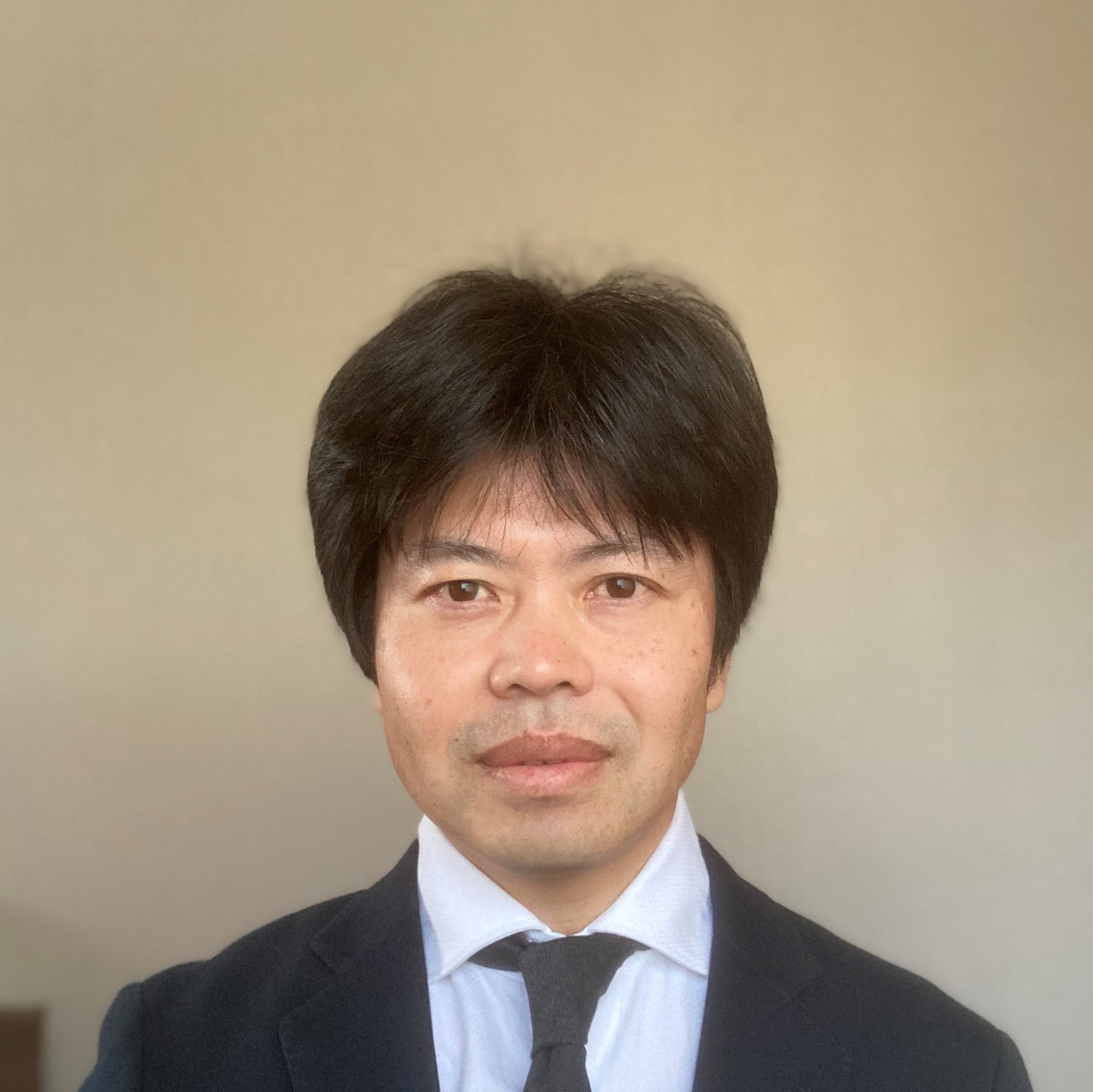
Keynote 1: Dec 12th, 2022, Grand Ballroom, 10:30 AM - 11:15 AM

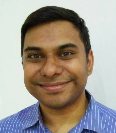
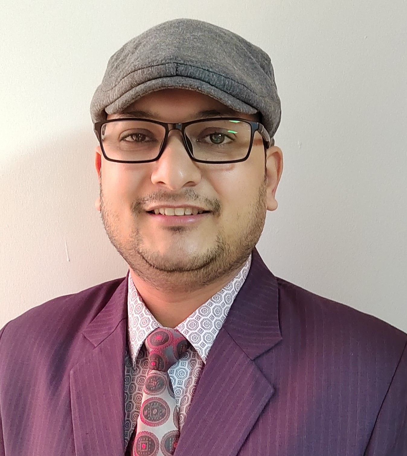
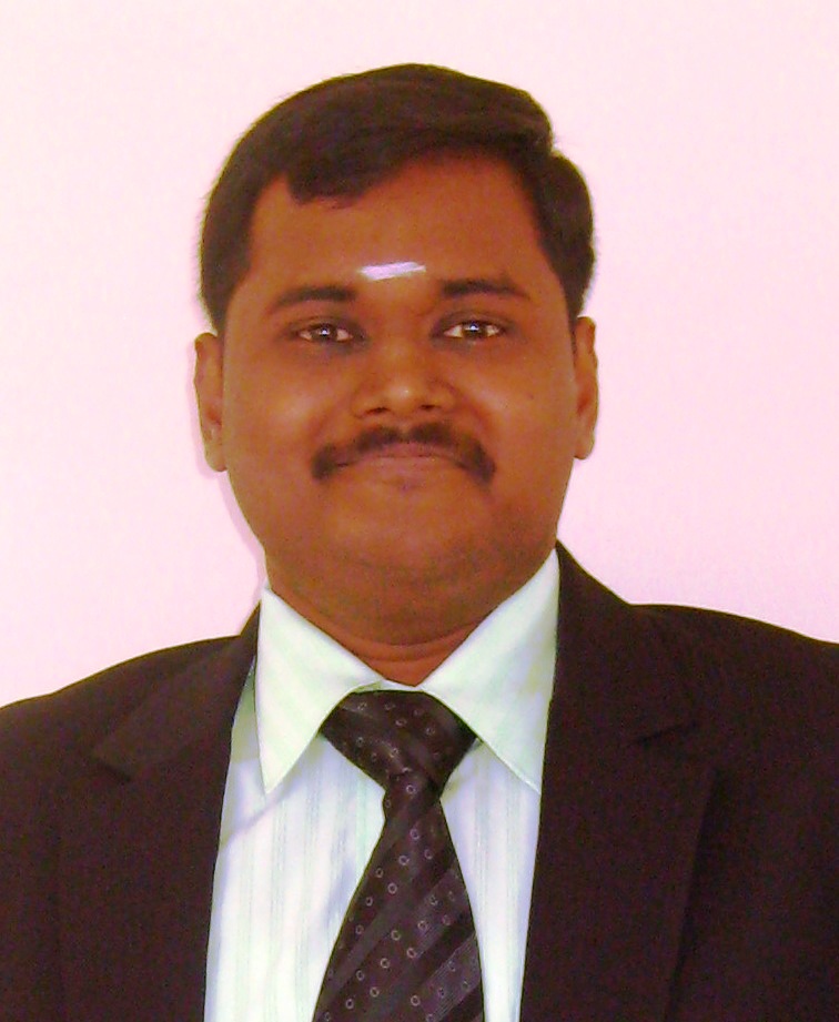
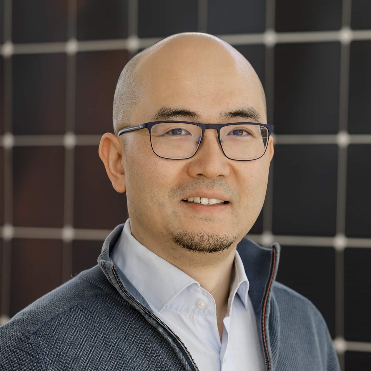
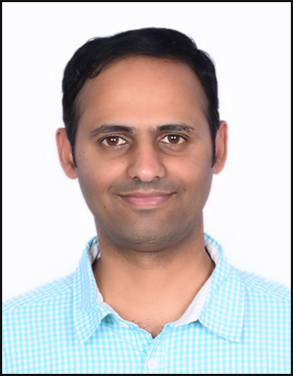
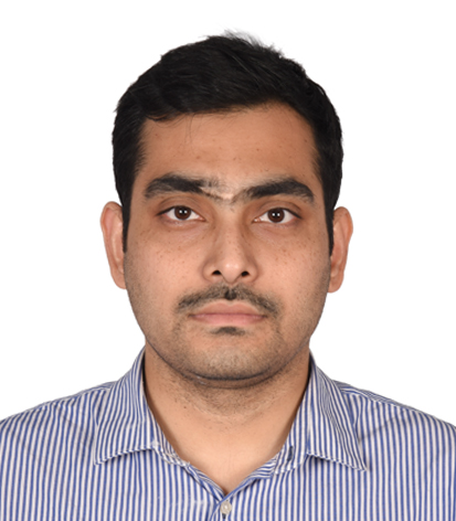
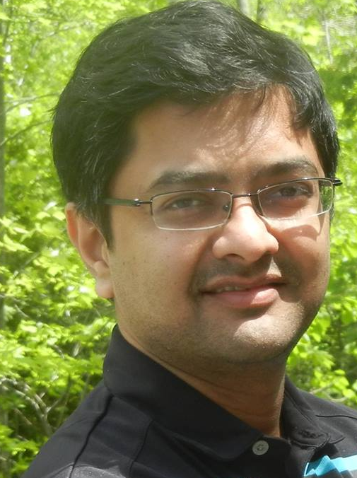
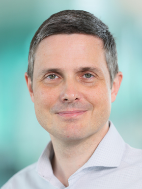
Speaker: Dr. Julio Costa (VP RF, Technology and Innovation, Global Foundries, Santa Clara CA, USA)

Title: RFSOI Technology for the RF Front-End: Then, Now and Tomorrow

Abstract:  RFSOI technologies are used today in the RF section of all cellular handsets, performing a number of different critical RF switching and tuning functions, and recently also providing an even larger number of low noise amplifiers, digital CMOS blocks and critical analog functions.    This talk will discuss the history of RFSOI technology, the critical enablers that allowed it to in a relatively short amount of time, completely replace the existing III-V switch technologies.   The progression to today’s modern RFSOI technologies and its array of device options will also be described, as well as future trends in RF switching technologies.  In particular, the RF front end of the future will incorporate a number of 3D technologies in both die-to-wafer and wafer-to-wafer bonding approaches in order to reduce critical dimensions while providing superior RF performance.

Bio:  Julio Costa was born in Sao Paulo, Brazil.  He is currently Vice President of RF Technology Development at Global Foundries in the Technology and Innovation Organization which he joined in 2022.  Previously he was a Senior Director of  Technology Development for QORVO in Greensboro, North Carolina, where he had been since 2002 leading a group of researchers focusing on Silicon SOI and RF MEMS technologies for next generation wireless systems.  He received his BSEE (1984) from the University of Wisconsin-Madison, and his MSEE (1987) and PHD (1992) from the University of Minnesota in Minneapolis.   He worked at Motorola Semiconductor Products  Sector (Freescale) from 1991 to 2001, where he worked as a researcher and technical manager in silicon and GaAs RF technology development.   He worked at ON Semiconductor until 2002, where he was a Director of R&D focusing on power management technology solutions.   He is the author of over 60 issued patents in the area of device and process technologies in RF, and has numerous publications and presentations.

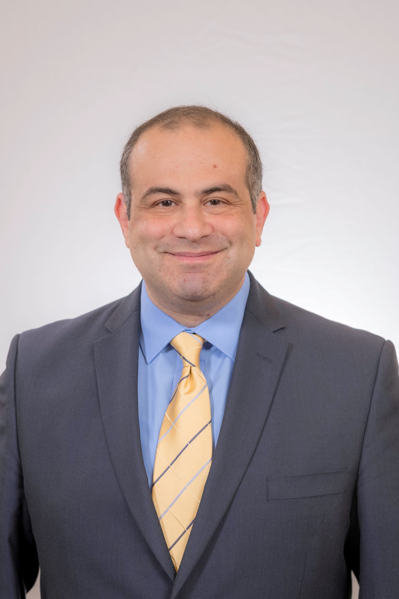
1

Keynote 2: Dec 12th, 2022, Grand Ballroom, 11:30 AM - 12:15 PM

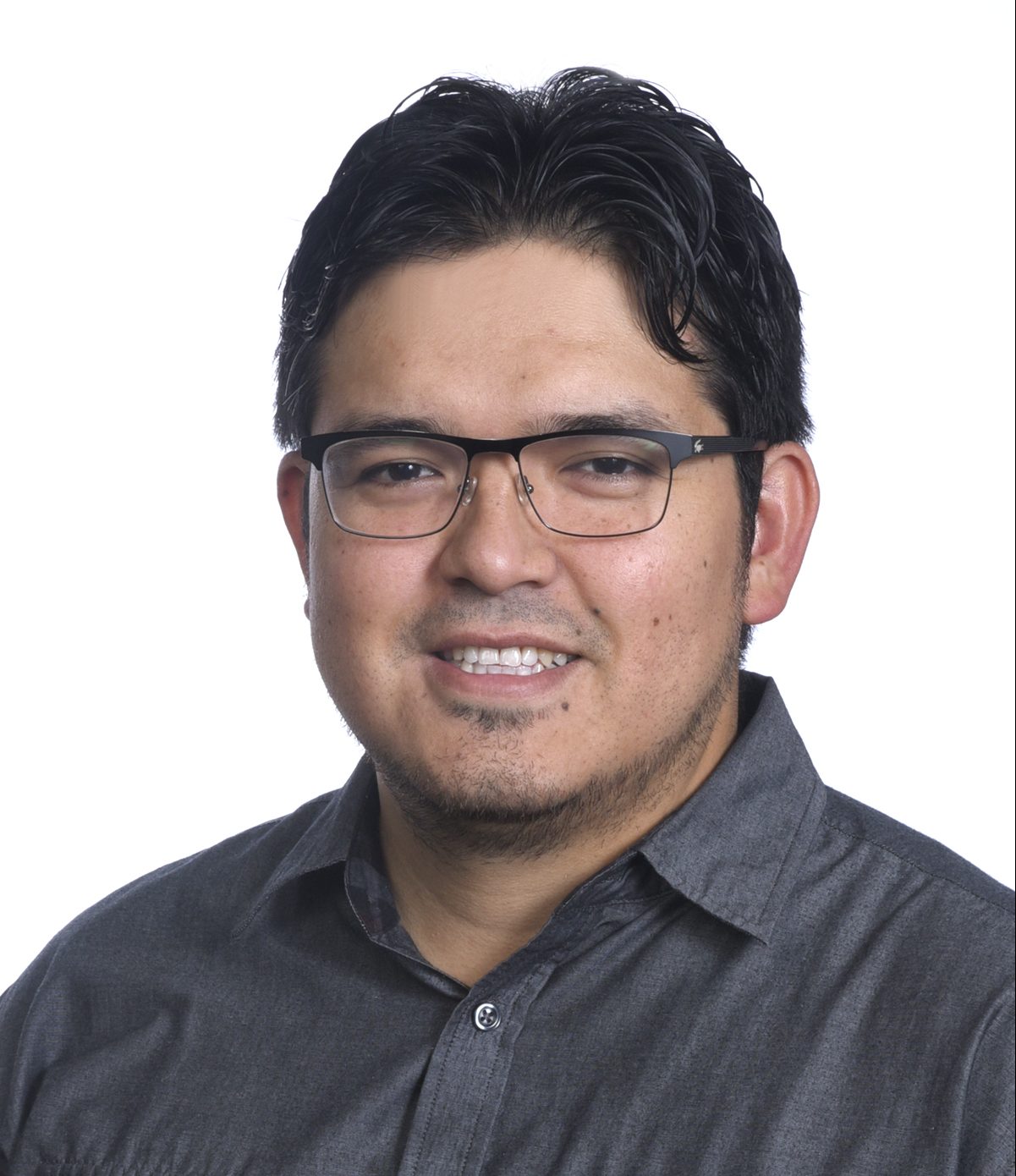
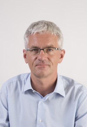
Speaker: Dr. Carlos Castro (Vice President & General Manager Nexperia, Germany)

Title: Power Semiconductor Technologies: a future pure WBG game?

Abstract:  The current power semiconductor market is still largely dominated by silicon-based devices. However, SiC penetration is growing very fast for new generation of systems and applications to come. Furthermore, with GaN offering significant benefits for increasing efficiency, power density and reducing cost, the question is if all three technologies will complement or replace each other. This presentation will reflect driving elements at different applications influencing the selection of technologies.

Bio:  Dr. Carlos Castro serves as Vice President and General Manager GaN for Nexperia and has more than 18 years of experience in power and automotive semiconductors. Prior to joining Nexperia, Carlos led the IGBTs/MOSFETs/SiC discretes business and automotive electronics activities at Littelfuse. Earlier he was in charge of Marketing and Application Engineering for automotive MOSFETs and led the Technical Marketing group for Electric Drive Train at Infineon Technologies. He has been granted several patents for power semiconductor devices and has been author of multiple papers and conferences presentations. Carlos holds a MSc and a PhD in Electrical Engineering from the Technical University of Dortmund, Germany and the University of Granada, Spain

2

Keynote 3: Dec 12th, 2022, Grand Ballroom, 12:15 PM - 1:00 PM

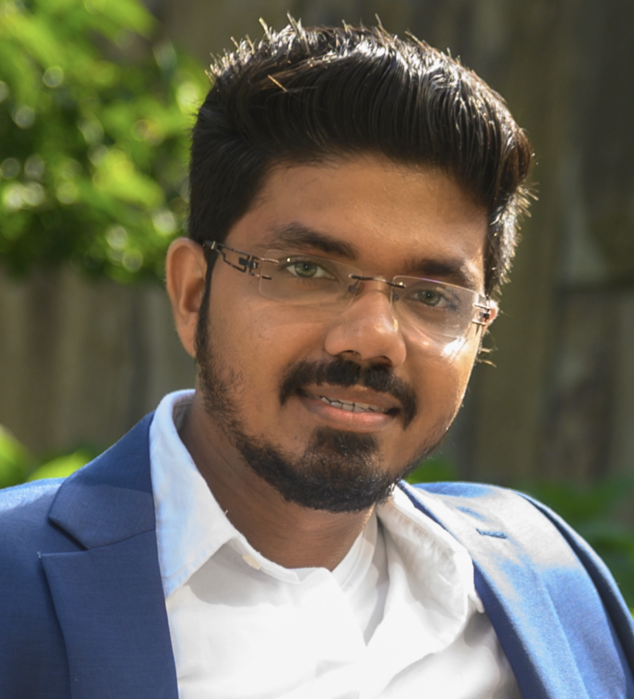
Speaker: Mr. Anand Ramamoorthy (Managing Director & Vice President, Micron, India)

Title: Memory at the Heart of Intelligence

Abstract:  As technology continues to be the key enabler of human development, data is at the heart of the new dynamics that is shaping our world.At the heart of this reimagined world is data, creating opportunity for new computing use cases and demanding new hardware foundations to feed applications faster and more efficiently. Memory and storage innovation drives that data hardware foundation that will unleash broadscale AI adoption, reshape data center computing, accelerate intelligent edge proliferation, and enable user experiences not yet imagined.The memory hierarchy is seeing a significant evolution where trends such as very large AI systems, 5G and data movement, autonomous driving and edge intelligence amongst others, are fueling the need for refined and customized memory solutions – both for the DRAM as well as the storage applications.  We are also seeing changes in the compute paradigms to recognize this evolving data centric model, leading to the emergence of new protocols.  All these together pose a complex set of challenges to memory solutions across the board in terms of technology, materials, packaging and systems. In this talk, we will dwell on these trends and we will talk about some of the exciting opportunities that are in front of us to enable the next generations of memory.

Bio:  Anand Ramamoorthy is currently Vice President and Managing Director at Micron India. In this role, he is charted to lead and drive one of the fastest ramps in engineering, R&D, services, sales and operations in India (across sites) for a $27B+ global leader in memory and storage solutions. In less than 3 years, Micron has more than quadrupled its headcount in India and has become a key contributor to Micron’s top line and bottom line. Anand is a seasoned, well-rounded technology executive with 22+ years of global experience building teams, scripting strategies, facilitating change management, growing business and leading organizational transformation. Anand joined Micron from McAfee (an Intel company, formerly Intel Security) where he was Managing Director of South Asia region. Prior to McAfee, Anand led South Asia consumption business at Intel where he resurrected their government business, incubated their mobile/tablet business from scratch and led the fastest growth in data centers among all regions in APAC. Anand started his career in Silicon Valley as a ‘hands on’ chip designer before moving on to roles of increasing impact and mandate including global GM roles with full P&L responsibility. After spending 10+ years in the US, Anand moved back to India 12 years back. Anand obtained his undergrad degree in Engineering from IIT (Roorkee) followed by M.S and MBA degrees from leading US universities. Anand is a frequent speaker at industry events (NASSCOM, CII, Zinnov, DSCI), actively mentors’ entrepreneurs and enjoys strong relationships within the CxO ecosystem in India. He is on the board of several companies including unicorns and large multinationals and works closely with industry bodies. He is an active media contributor and has featured in the very popular ‘Young Turk” program that aired on CNBC India. Anand is part of Telangana government’s advisory council and actively collaborates with NITI Aayog, MEITY, Invest India, WEF and other key central government organizations. Anand is married to Revathi and they have a son (Arnav). He is an avid reader, prefers mostly non-fiction/biographies, and enjoys playing tennis with his son.

3

Keynote 4: Dec 13th, 2022, Grand Ballroom, 10:00 AM - 10:45 AM

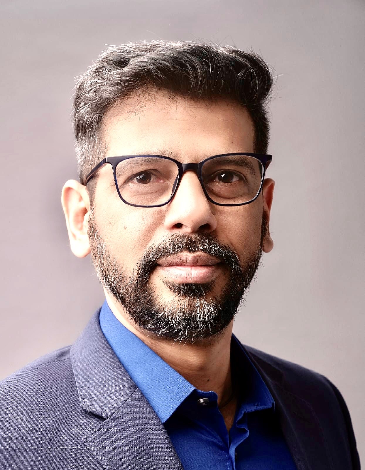
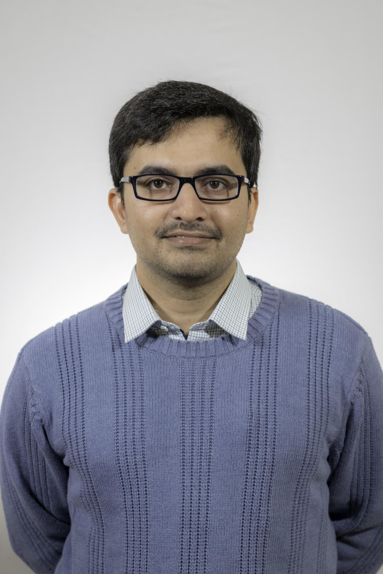
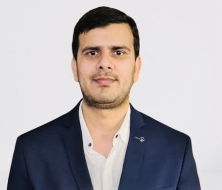
Speaker: Dr. Primit Parikh (Co-Founder & President, Transphorm Inc., USA)

Title: Manufacturing and Commercialization of Easy to Use, Robust, High Performance GaN Power Devices – from 650V to 1200V, from 45W to 10kW+

Abstract:  GaN technology needs to serve the broadest market to be a viable solution in the long term. Transphorm’s robust normally-off GaN FET with its integrated Si-GaN architecture provides easy to interface, highest performance solutions with the best in class proven reliability with over 80 billion hours in the field: from low wattage markets such as adapters/chargers through Titanium-class power supplies to Renewable Energy to Electric Vehicles solutions such as on-board chargers and DC/DC converters today and traction tomorrow. With its vertically integrated wafer manufacturing providing control, scale and rapid innovation backed by one of the strongest IP portfolio in GaN power, Transphorm provides the GaN industry’s first 650V and 900V AEC-Q101 product with 1200V in its roadmap. This presentation will detail how Transphorm’s GaN solutions enable our customers to serve the broadest and fastest growing power conversion markets – from low power to high power, from adapters to automotive as well as GaN manufacturing, including in the context of India’s Semiconductor Mission

Bio:  Primit co-leads Transphorm, a pioneer and leader in GaN Power Semiconductors. Having recently led Transphorm to a public company listing partnering with it’s phenomenal team, he is passionate about creating value from the intersection of business and technology.  With over 20 years of semiconductor & entrepreneurial experience, his background includes capital raises, international markets & strategic partnerships, key customer relationships, products & manufacturing, IP, GaN/Semi technology and government contracting. Prior to Transphorm, Primit led GaN electronics at Nitres Inc. through its acquisition by Cree, where he served as the head of Advanced Technology at Cree SBTC in charge of GaN development and government business. Primit received his B.Tech. in EE from IIT, Mumbai and his Ph.D. in ECE from UCSB. He has more than 40 patents awarded and co-authored more than 75 publications and presentations. He is blessed to reside in the amazing Santa Barbara area with his wonderful family.

WhatsApp Image 2022-09-16 at 1.27.54 PM

Keynote 5: Dec 12th, 2022, Grand Ballroom, 10:00 AM - 10:45 AM

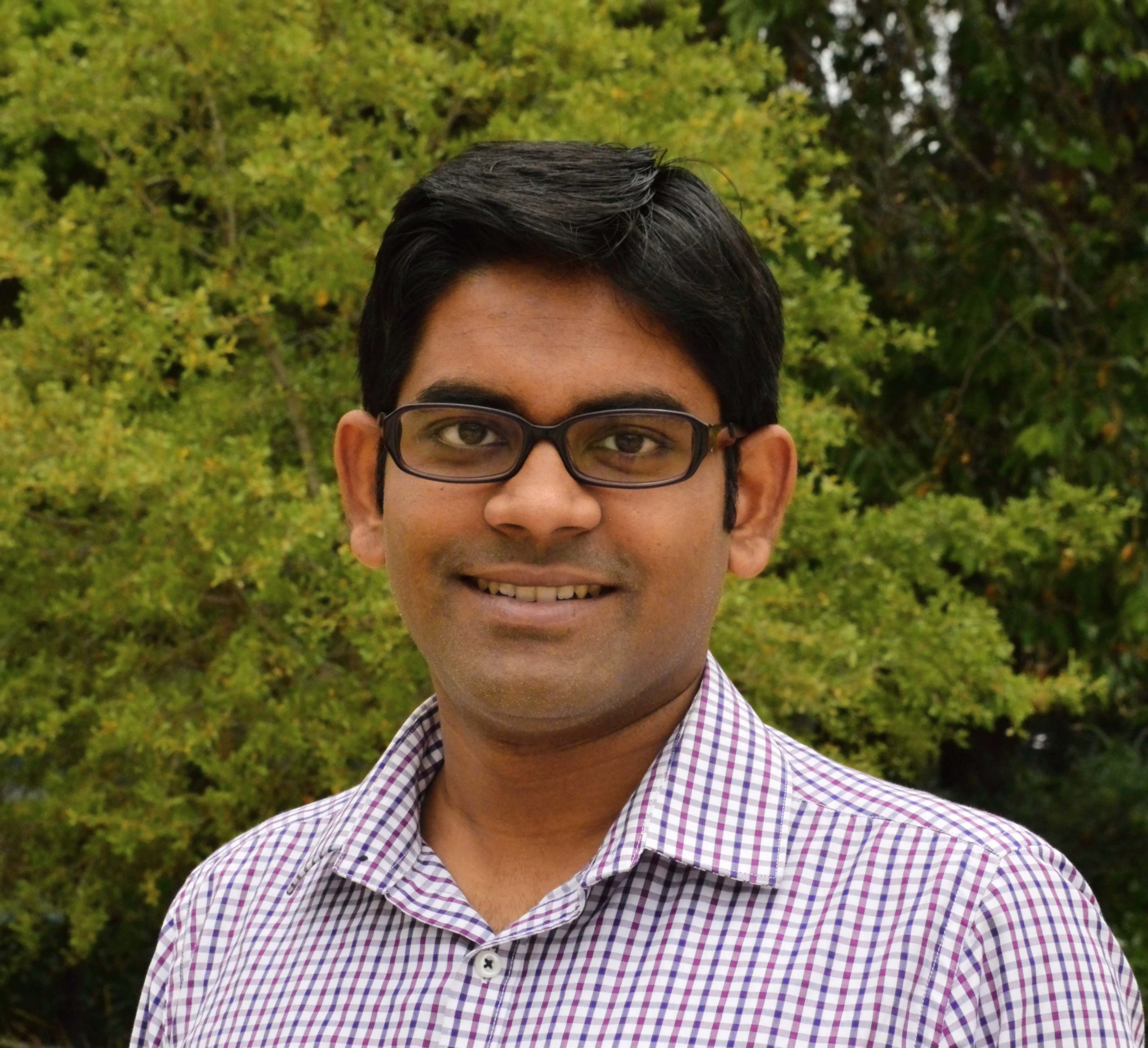
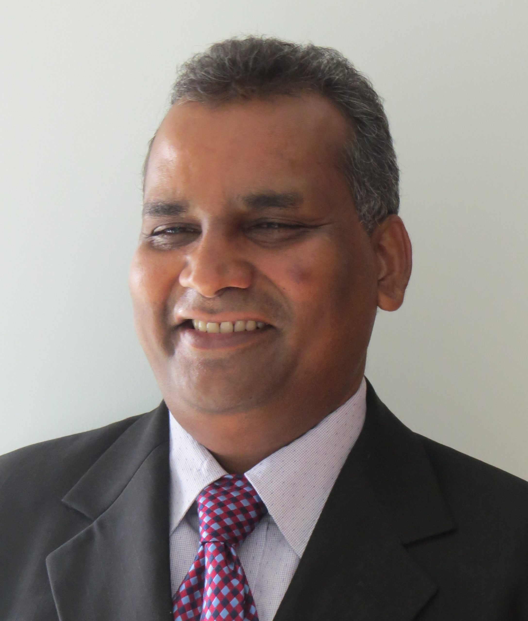
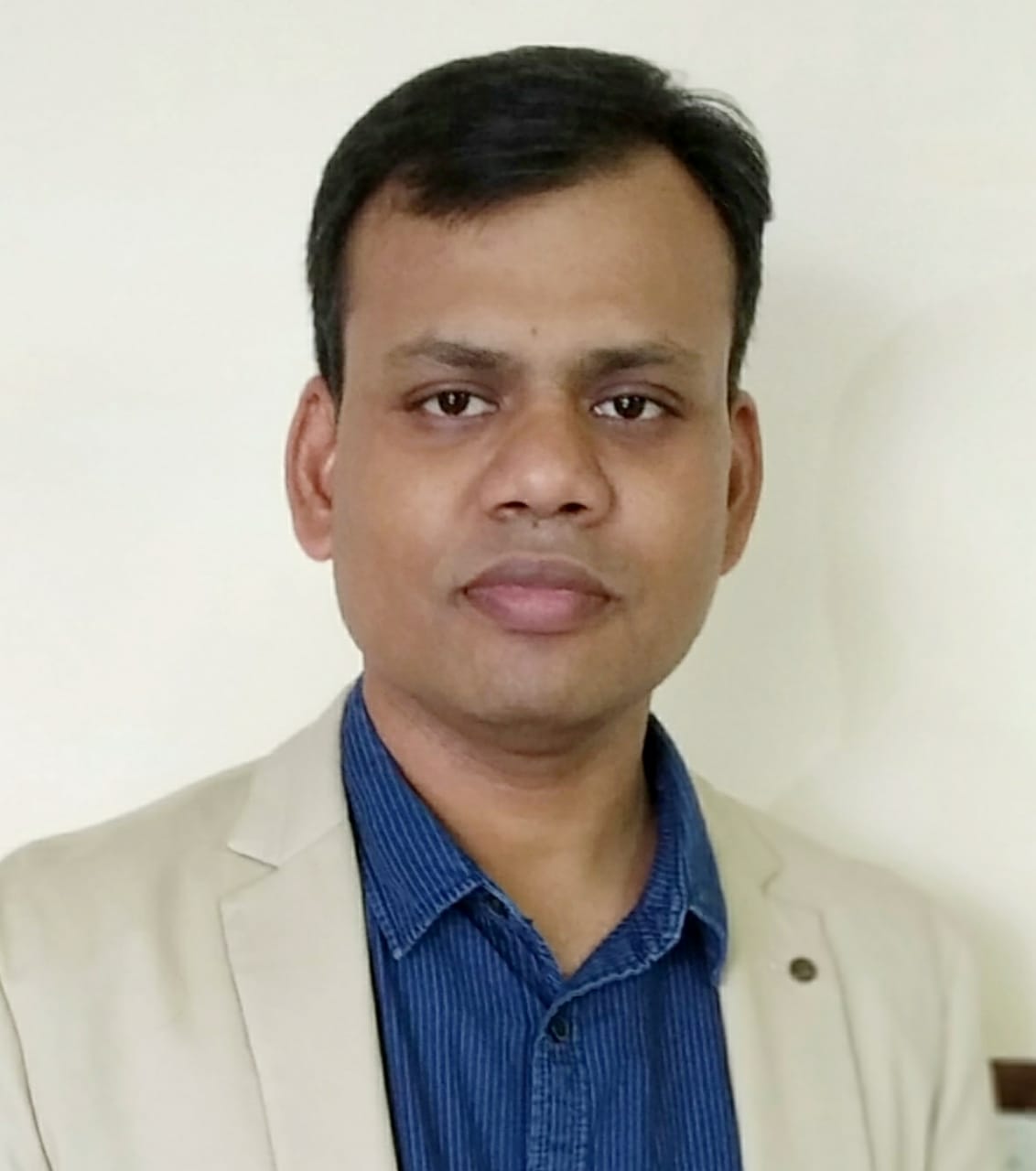
Speaker: Dr. Milind Kulkarni (President, PV Manufacturing, Reliance Industries, India)

Title: Solar Value Chain: Historical Evolution, Technology platforms, and Roadmap

Abstract:  Solar energy has become commercially attractive on the foundation of semiconductor polysilicon, crystal, and wafer processing technologies, complemented by the emergence of efficient cell technologies founded on unit operations well-established in the semiconductor industry. These technology platforms will further push product performance and can deliver module cash cost less than $0.12/W and LCOE less and $0.02/kWh (DC) over the next 5-year horizon. In addition, more attractive new technology platforms are emerging. This talk focuses on both technical and commercial aspects of the solar value chain and opportunities ahead

Bio:  Milind Shrinivasrao Kulkarni brings uniquely broad expertise in essentially all relevant disciplines of business, including General Management, Technology, Strategic Analysis, Business Development, Mergers & Acquisitions, Finance, Marketing, Operations, and Supply Chain. He has extensive background in solar silicon processing from Polysilicon Production to Module Assembly and in semiconductor silicon processing from Crystal Growth to Silicon Epitaxy. His cross functional expertise enables him to contribute to various business sectors. Milind has extensively worked in both the US and India. His geographical business exposure is even broader, covering many countries in the northern hemisphere. Milind is serving as President of PV manufacturing in Reliance New Energy Solar, where he is responsible for setting the business vision and executing the overall Solar and PV business plan. He oversaw cell and module technology development and implementation as the CTO of Vikram Solar, before joining Reliance. From July 2017 to February 2021, Milind served as the CEO of Suzlon Renewable Technologies and its sister company, Svagos Technik, where he was responsible for the development of next generation semiconductor and renewable technologies and implementation of these technologies in HVM. Milind’s prior experiences were in the entire solar and semiconductor value chains in MEMC Electronic Materials, SunEdison, and GCL-Solar Materials, all part of one family of companies with a common origin. Milind led (as the CTO and VP/EVP of Strategic Expansions) Technology and Strategic Expansions in SunEdison-Solar Materials and later GCL-Solar Materials, which was the materials technology division of SunEdison before its acquisition by GCL. Milind worked on developing collaborative and strategic business partnerships (JVs) to implement SunEdison’s Polysilicon, Crystal Growth, Wafering, and Module technologies into HVM. He was also responsible for explorative development of solar cells with various collaborators. He oversaw the development of turnkey solutions from technology selection to HVM. He represented SunEdison’s interests as a member of the Board of Directors of SunEdison’s polysilicon production joint venture with Samsung Fine Chemicals, SMP. In the past, Milind also directed sales and operations management, demand and supply forecasting, capacity and inventory management, supply chain mapping and optimization, operations research and production optimization, lean initiatives, and technology driven procurement across the solar materials value chain, along with cross-functional quantitative research in the entire semiconductor and solar value chains. Milind and his teams have developed new technologies that can create more than $10 B in value. Milind also facilitated M&A activities valued more than $100 M. Milind is an author or co-author of more than 70 international journal publications, patents, conference presentations, invited plenary talks, and book chapters, collectively. He also started the Solar Silicon Symposium in China (2009) that has grown into China Photovoltaic Technology International Conference (CPTIC). Both his doctoral work and industrial research have received special recognitions by The AIChE Journal (Paper of the Month) and The Journal of The Electrochemical Society (Technical Highlight). Milind actively served as an official reviewer for various journals. He was a member of the Editorial Advisory Board of The Industrial and Engineering Chemistry Research (an ACS publication) and served as a member of The National Council of Engineering School of Washington University, St. Louis, USA. Milind holds a bachelor’s degree from University of Mumbai (ICT/UDCT), master’s degree from Oregon State University, doctorate from Washington University, all in chemical engineering. He also holds a master’s degree in business administration, from Washington University. Milind won the Alumni Achievement Award of Washington University in 2012. For details, visit the following websites: https://engineering.wustl.edu/offices-services/alumni/McKelvey-Engineering-Award-Years/2012.html


Prof. Prashant Murlidhar Sonar

Queensland University of Technology

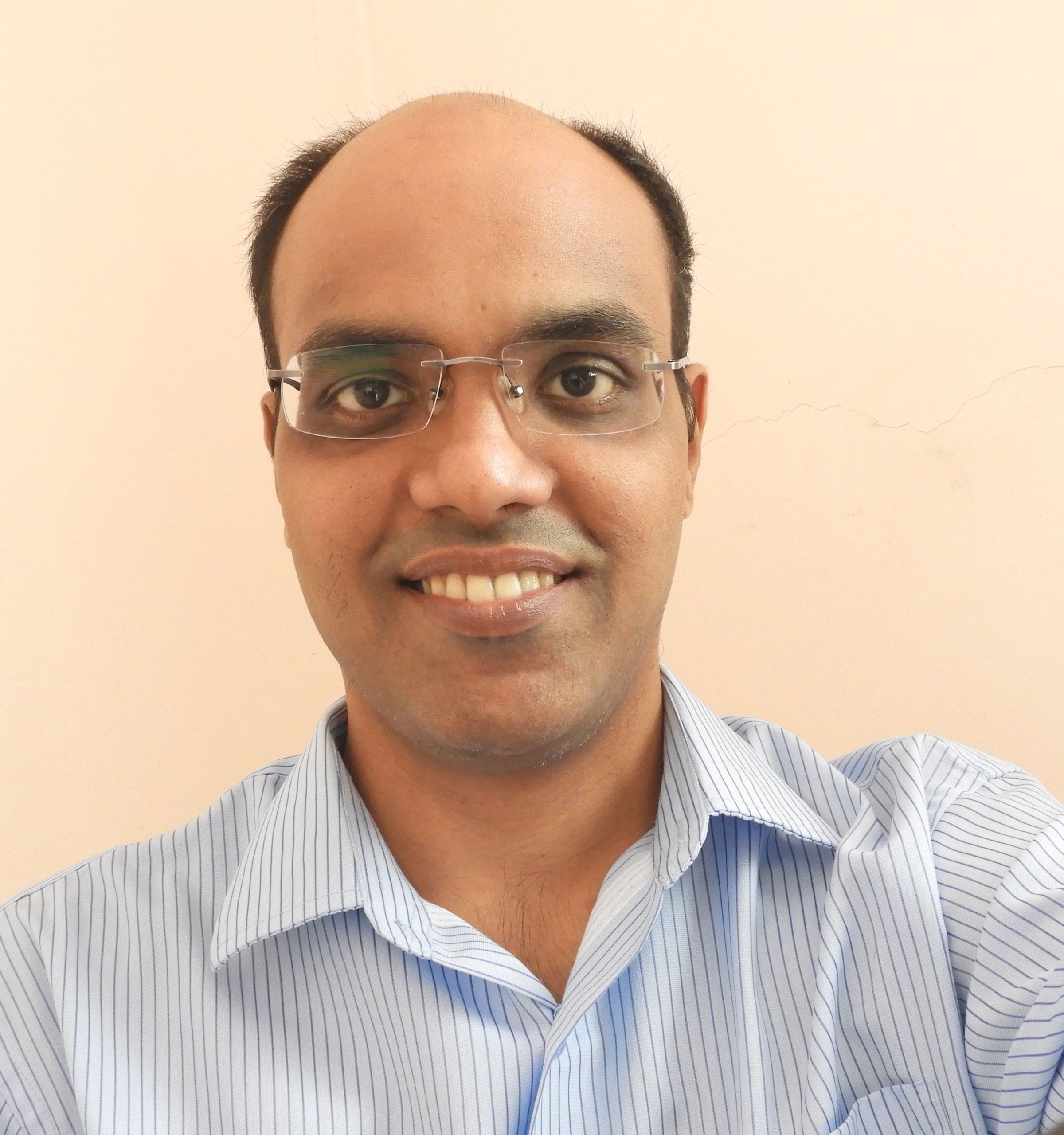
Bio: Prof. Prashant Sonar is an ARC Future Fellow and Professor in the School of Chemistry and Physics and Centre for Material Science at the Queensland University of Technology, (QUT), Australia. He is serving as an Associate Editor of the journal Flexible and Printed Electronics and Material Research Express (Institute of Physics, London). Recently, he has been elected as a Fellow of the Royal Chemical Society (FRSC) and a Foreign Fellow of the Maharashtra Academy of Sciences (FFMAS). He is a recipient of the Award for Excellence-Impact and Translation (2020), from the Centre for Materials Science, QUT, Australia, and the Vice-Chancellors Performance Award from QUT Australia (2016). He also received Thiemann Exchange Program Award from Technion-Israel Institute of Technology (2017), Israel, and the Foreign Collaborator Award from Grant-in-Aid for Scientific Research on Innovative Areas, MEXT, (2016) Japan. He has published 225 peer-reviewed research papers (H-index-51, close to 10,000 citations) and filed 3 US patents. Prof. Sonar delivered 90 invited talks at international conferences and institutes.

Talk Title:  Molecular Engineering of π-Functional Conjugated Materials for Photonics, Electronics, and Sensing

Abstract: Next generation active electronic materials used in devices are undergoing continual improvements to generate devices that are high performance, lighter, flexible, stretchable, and more energy efficient with lower cost. Carbon based novel solution processable π-functional conjugated materials are the focus of intense academic and industrial research since they are important class of soft materials for large area electronics including transistors, displays, sensors and light harvesting devices. The active organic semiconducting materials are emerging due to their tunable light absorption/emission, interesting charge transport properties, relatively adequate HOMO-LUMO energies and ink formulation capability.
In my talk, I will explain the various classes of conjugated carbon-based materials either as polymers, small molecules or quantum dots prepared via chemically and electrochemically using various novel aromatic conjugated building blocks. In this presentation, the design, synthesis, optoelectronic properties, and device performance of novel advanced materials for field effect/electrochemical transistors, perovskite solar cells, light emitting diodes, optical sensors and various sensing devices will be discussed. Such materials and devices have great potential in future electronics, energy, health, and environmental monitoring.

Prof. Shreepad Karmalkar

IIT Bhubaneswar (at the time of presentation)

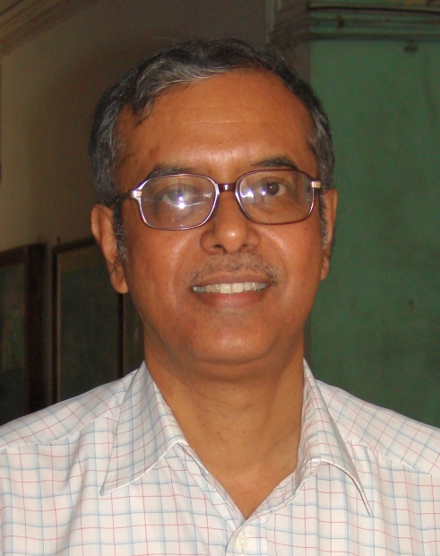
Bio: Shreepad Karmalkar is a Professor of Electrical Engineering at IIT Madras. He received the B. Tech and accelerated PhD degrees in Electrical Engineering from IITM, in 1983 and 1989, respectively. His interests are semiconductor devices and education. His recent devices related research has focused on modeling and simulation of power devices, nano-devices, GaN HEMTs and solar cells. He has developed popular online video courses on Solid State Devices, Semiconductor Device Modeling and Introduction to Research. 

Talk Title: Modeling and Design of Superjunctions in Silicon Carbide

Abstract: Superjunctions yield a lower specific on-resistance, RONSP, for a given breakdown voltage, than conventional p-n junctions. We derive (a) a new theoretical lower limit of RONSP for an ideal balanced superjunction that is 30 % lower than prior works, (b) closed-form design equations for a practical superjunction considering process variations for the first time, and show that the optimum p-pillar aspect ratio is < 15 whereas prior works have tried raising this ratio beyond 25. We also propose charge sheet superjunction as a viable alternative to superjunction in SiC material to avoid complexities associated with fabrication of p-pillars in SiC.

Prof. Shankar Kumar Selvaraja

Indian Institute of Science

Bio: Professor Shankar Kumar Selvaraja is Prof. RamakrishnaRao chair associate professor at CeNSE, IISc Banglaore. He is the current Chair of the National Nano fabrication Centre (NNfC) at IISc. Before joining IISc, he was with imec Belgium. His current area of research includes silicon photonic IC enabled optical connectivity technology, integrated photonic based sensors, neuromorphic photonics and quantum photonic integrated circuit. He has published over 250 research articles in international journals and conferences and has six international patents.

Talk Title: Silicon and silicon nitride photonics for sensing and communicaiton 

Abstract: In this talk, we shall discuss the strategies to integrate silicon and silicon nitride to create a broadband photonics platform. We shall discuss material requirement, device design, fabrication challenges and measurement results of detectors for potential sensor and high-speed communication applications. 

Prof. Steven Ringel

The Ohio State University, USA

Bio: Steven A. Ringel is a professor and holds the Neal Smith Endowed Chair in the Department of Electrical and Computer Engineering at Ohio State. He is also the Founding Director of The Ohio State University Institute for Materials Research (IMR), which encompasses Ohio State’s multi-college materials research enterprise spanning 6 colleges, more than 140 faculty groups, and both government and industry-supported centers of research excellence. Prof. Ringel is an internationally recognized authority for his research innovation and leadership in electronic materials and devices, and particularly for his pioneering contributions that are advancing high efficiency and low-cost compound semiconductor-silicon integrated photovoltaics and also for his efforts to advance wide bandgap electronic and photonic device technologies through the development and application of several defect characterization methods.

Talk Title: Investigation and Comparison of Deep Acceptors in β-Ga2O3 using Defect Spectroscopies

Abstract: Steven A. Ringel(1), Hemant Ghadi(1), Joe F McGlone(1), Alexander Senckowski(2), Shivam Sharma(3), Man Hoi Wong(2) and Uttam Singisetti(3)
(1) Electrical and Computer Engineering, The Ohio State University, Columbus, Ohio,
(2) Electrical and Computer Engineering, University of Massachusetts Lowell, Massachusetts,
(3) Electrical Engineering, University of Buffalo, Buffalo, New York
Beta phase gallium oxide (β-Ga2O3) is a strong contender for next-generation high voltage and RF device applications. A key component of such devices is a semi-insulating, highly resistive buffer layer or substrate. To date, iron (Fe) has been the preferred acceptor impurity to achieve semi-insulating β-Ga2O3. Iron produces an energy level at EC-0.8 eV, which has been substantiated by theoretical and experimental studies and enables highly resistive material. However, it has also been shown that residual Fe impurities can result in device switching instabilities since the Fermi level can modulate the occupancy of the Fe trap state during standard biasing conditions. While progress to mitigate the impact of residual Fe impurities has occurred, there is also interest in exploring acceptors with much deeper energy levels to avoid device instabilities. Magnesium (Mg) and nitrogen (N) have emerged as candidates based on their predicted energy levels of EC-3.3 eV and EC-2.8 eV, respectively (H. Peelaers, et al., APL Mater. 7, 022519, 2019). This presentation will compare each acceptor, with a primary focus on N, using deep level optical spectroscopy (DLOS) and thermally based deep level transient spectroscopy (DLTS).
Here, N acceptors were introduced into HVPE-grown β-Ga2O3 by ion implantation. A uniform N-implantation profile was used targeting multiple doses in different samples, followed by an activation anneal. DLTS and DLOS measurements were applied before and after annealing. After implantation, multiple trap states appeared, most of which were removed by annealing, leaving a single, new state at EC-2.9 eV, with a Frank-Condon energy of 1.4 eV. The concentration of this state monotonically tracked with nitrogen concentration from SIMS. This energy level closely matches predicted values for an acceptor-like defect due to nitrogen atoms occupying the oxygen III sites, determined by density functional theory (DFT) calculations (H. Peelaers, et al., APL Mater. 7, 022519, 2019; Y.K. Frodason, et al. J. Appl. Phys. 127, 075701, 2020), The much deeper energy compared with Fe could imply a significantly lower operational instability than the shallower Fe acceptor at EC-0.8 eV. However, we found that the below midgap position of the NO(III) level, coupled with its small optical cross-section, complicates the trap concentration analysis by DLOS, which is important for understanding how to characterize very deep states in β-Ga2O3. Simultaneous hole emission to the valence band and electron emission to the conduction band was seen. Similar challenges might be present for Mg doping as well. The impact of this behavior on DLOS analysis is discussed, and a method to resolve this complication will be presented, which is needed to guide further optimization of this critical step in gallium oxide device development.

Dr. Anton Devillier

Tokyo Electron Ltd; USA

Bio: Anton, born in Oregon, moved to South Africa where he completed his undergraduate degree at the University of Cape Town. After returning to America, he completed his studies at the University of Oregon. He has many years of experience working for top companies along the way – starting at Hyundai Semiconductor, moving to Maxim, Cypress Semiconductor, and Micron, and now holds the position of VP of Patterning Technology at TEL. His work at TEL includes logic scaling analysis with the development of many scaling boosters and patterning strategies to extend scaling through integration.

Talk Title: Not given 

Abstract: Over the last 20years or so the industry scale path has seen many transitions to enable what each preceding generation of technology thought was impossible. New technology becomes possible with the addition of patterning techniques that help enable each generation of smaller designs. This talk will go through some of the enabling technologies and how the industry of chip making made breakthrough after breakthrough to truly enable parts to be printed at dimensions and geometries far more exotic than any could have imagined. We will take a look at the recent history of technology scaling enablers and how they shaped the industries roadmaps and understanding of scaling. 

Dr. Abhinav Kandala

IBM Quantum, USA

Bio: Dr. Abhinav Kandala is an experimental physicist and manages the Quantum capabilities and demonstrations group at IBM Quantum. At IBM, his research has spanned coherence and control of superconducting qubits, multi-qubit device characterization, and applications of near-term quantum computers. Abhinav received his B. Tech in Engineering Physics from IIT Bombay and a PhD in Physics from The Pennsylvania State University. In 2019, he was recognized as on one of 35 innovators under 35 by MIT Tech Review.

Talk Title: Error mitigation and the path to quantum advantage

Abstract: Quantum processors based on superconducting circuits have now reached a scale that is well beyond direct diagonalization. However, in the absence of fault tolerance, the central question is whether such noisy processors can provide useful computations. In this context, error mitigation techniques can provide access to noise-free observables even from today’s noisy processors. I will introduce these techniques, discuss the current state of quantum hardware and recent experimental results, and chart out an immediately accessible path to quantum computational advantage.

Dr. Dhananjaya Dendukuri

Achira Labs, India

Bio: Dhananjaya Dendukuri is Chief Executive Officer & Co-Founder of Achira Labs, a pioneering point-of-care technology company based out of Bangalore. Dhananjaya returned to India with his passion for engineering and the belief that technology development for underserved markets must be done locally. Starting from his early career experience as a lab scientist and R&D manager (with over 30 publications and 7 issued patents), he now has more than a decade of experience with the fund-raising, commercial, operational and regulatory aspects of building and taking diagnostic technologies to market. He received the National Technology Award for new technologies (biotechnology) in 2016 and MIT Technology Review’s prestigious TR35 awards in India for the work that was being done at Achira. Dhananjaya serves on the jury of the Infosys Prize and the X-prize for diagnostics. He received his PhD in Chemical Engineering from MIT, a MASC in Chemical Engineering from the University of Toronto and a B.Tech in Chemical Engineering from the Indian Institute of Technology, Madras.

Talk Title: Hydrogel based sensors for medical diagnostic applications

Abstract: Synthetically fabricated hydrogel particles are increasingly used for bio sensing applications. Newly developed techniques allow fabrication of hydrogels with different morphologies, spatially segregated functionalization and tuned material properties. Hydrogel sensors embedded inside microfluidic devices have a number of advantages including multiplexing, good stability and low non-specific binding. The talk will discuss hydrogel sensor capabilities on Achira’s point-of-care platform. 

Seena V

Dr. Seena V

Indian Institute of Space Science and Technology (IIST), India

Bio: Dr. Seena.V received Ph.D. from the IIT Bombay in 2011. She served as a faculty member at IIT Jodhpur and R& D Consultant for NanoSniff Technologies Pvt. Ltd., incubated at IIT Bombay partly based on her research contributions in Microcantilever sensors. She is currently an Associate Professor in the Dept. of Avionics, Indian Institute of Space Science and Technology (IIST). Her main research is in the area of MEMS and CMOS-MEMS integration and Nanomechanical Sensor Systems. She is a recipient of NASI Young Scientist Platinum Jubilee Award, Kerala State Young Scientist Award, SERB Women Excellence Award ,Award for Excellence in Ph.D Thesis, IIT Bombay” and IEI Young Engineer Award .

Talk Title: MEMS Physical Sensors with Integrated FET based Electromechanical Transduction

Abstract: MEMS sensors and devices have numerous applications spanning across consumer gadgets, automotive electronics, industrial medical, defence, aerospace etc. Despite the wide and increasing demands for MEMS-based devices such as sensors and actuators in diverse applications, unlike semiconductor technologies like CMOS/VLSI, the design and fabrication of MEMS/Microsystems is not fully standardized. Most of the commercially available MEMS sensors are based on passive transduction mechanisms such as capacitive or piezoresistive with inherent performance limitations. FET based active transduction schemes have the potential to overcome these limitations with ease in CMOS-MEMS integration as an additional merit. This talk would give a brief overview of our attempts towards indigenous development of MEMS physical sensors with FET based electromechanical transduction with scope for CMOS-MEMS integration. 

D S Prasad

Dr. Duvvuri satyanarayana Prasad

Centre for Materials for Electronics Technology (C-MET), Hyderabad, India

Bio: Dr D S Prasad, Ph.D in physics, working as scientist in a Research & Development organization C-MET, Govt. of India. He had 25 years of hands-on experience in the refining of materials to purities of 99.99% (4N) through 99.99999% (7N). Skilled with the related aspects of purification technology, material handling and purity verification. Currently, he is in-charge for the activity “Recycling of end- of life silicon-Solar PV modules” supported by MeitY, Govt. of India

Talk Title: A novel approach for recycling of waste silicon solar photovoltaic modules: A step to promote circular economy

Abstract: With the average lifespan of a solar module being 25-30 years, it is predicted that the cumulative waste generated globally would be around 78 million tonnes by 2050. Hence, developing a process for the recycling of this solar waste is crucial to prevent environmental pollution and to recover valuable materials. It is important that the end-of-life of solar modules should stay green to maintain the circular economy. Our work is focused on the recovery of valuable materials from spent crystalline silicon solar modules by a combination of physical, chemical, and thermal operations to de-laminate the modules and purify the materials. Through this process, an economically viable method was established to recover high pure silicon along with other components such as glass, copper etc.

Prof. Doron Naveh

Bar-Ilan University, Israel

Bio: Doron Naveh earned his BSc in Materials Engineering, as well as a BSc and MSc in Physics from Ben-Gurion University of the Negev, and his PhD in Computational Materials Science from the Weizmann Institute of Science. In 2008 he moved to Princeton University and in 2009 to Carnegie-Mellon University for post-doctoral fellowships, where he started the transition from computational to experimental sciences. In 2012 he started the 2D Materials & Devices Lab in the Bar-Ilan Facultyof Engineering, where he is now an Associate Professor.

Talk Title: From Enhanced Responsivity to Deep Sensing: Advances in Light Detection

Abstract: 

The emergence of 2D layered compounds has ameliorated the fields of electronic and optoelectronic devices and are considered as a promising platform for the developments of devices in the quantum era. To list a few examples, this progress has included the demonstrations of ultrafast photodetectors, room-temperature mid-infrared photodetection, and electrical tunable spectral response by Stark effect. In this talk the recent progress on combined trajectories will be discussed – including fast, room temperature short wave infrared detection of hot photo carriers by intercalated MoS2 and a few examples on the electrical control of spectral response in photodetectors of 2D materials and heterostructures. Finally, the use of computational resources for the performance of spectral measurements, termed “Deep Sensing”, will be shortly reviewed.

References

[1] A. Twitto et al. ACS Nano 2022 https://doi.org/10.1021/acsnano.2c07347

[2] C. Stern et al. Advanced Materials 2021 https://doi.org/10.1002/adma.202008779

[3] S. Yuan et al. Nature Photonics 2021 https://doi.org/10.1038/s41566-021-00787-x

Prof. Sukomal Dey

Indian Institute of Technology Palakkad

Bio: Sukomal Dey received Ph.D. degree from the Indian Institute of Technology Delhi, New Delhi, India, in July 2015. From August 2015 to July 2016, he was a Project Scientist with Industrial Research and Development Centre, IIT Delhi. From August 2016 to June 2018, he was with National Tsing Hua University, Taiwan, as a Post-doctorate Research Fellow. Since June 2018, he has been an Assistant Professor with the Department of Electrical Engineering, Indian Institute of Technology Palakkad, India. 

Talk Title: Radio Frequency Micromachined Devices and Circuits for Microwave to millimeter Wave Applications

Abstract: When radio frequency microelectromechanical system (RF MEMS) based switches appeared more than 25 years ago, micromechanics have attracted huge attention for enabling near-ideal microwave devices. Since then, MEMS switches and circuits went through different development stages and are currently proving themselves commercially. Micromachining technology has the potential to become an enabling technology for microwave, millimeterwave to even sub-millimeterwave systems. Although, reliability of MEMS devices is one of the prime challenge to meet present state-of-the-art performances due to occurrence of multiple failure modes after few cycles of operations. This reliability becomes more critical when multiple MEMS switches operate simultaneously like in a multi-bit digital phase shifters. First phase primarily concentrates on the reliability improvements on MEMS based switching networks and digital phase shifters. It takes multiple iterations and extensive characterizations to conclude with a reliable MEMS phase shifters. Second phase briefly presents development of tunable bandpass filters utilizing MEMS switches for present 5G applications. Third phase briefly shows the potential of micromachined antennas for phased array networks. Finally, present webinar concludes with current research activities of RF MEMS in sub-millimeterwave regime. 

Prof. Satyabrata Jit

Indian Institute of Technology (BHU) Varanasi, INDIA

Bio: Prof. S. Jit is a senior Professor in the Department of Electronics Engineering, Indian Institute of Technology (BHU) Varanasi, INDIA. He has supervised 31 Ph.D. theses and has published 198 journal articles (including 73 IEEE papers) and authored/coauthored/edited 06 books. Prof. Jit is an Editor of the IETE Journal of Research, Associate Editor of two journals: IET Micro & Nano Letters and Journal of Electronic Materials.

Talk Title: Modeling, simulation and applications of engineered TFETs

Abstract:  The tunnel field effect transistor (TFET) has drawn considerable attentions for future generation low-power VLSI/ULSI applications due to its extremely low sub-threshold current and good switching characteristics. The TFET possesses low sub-threshold swing below the Boltzmann limit of 60 mV/decade of the bulk MOSFETs. However, the major drawback of the TFET is its very poor ON current. Several techniques have been introduced to improve the performance of the TFETs through various structural modifications. The present talk will introduce the performance analysis of some engineered TFET structures via theoretical modelling and commercially available TCAD simulations. Finally, some applications of the engineered TFETs in the SRAM design and level-free bio-sensors will also be discussed.

Dr. Swaroop Ganguly

IIT Bombay, India

Bio: Swaroop Ganguly received the B.Tech. from IIT Kharagpur, and the Master’s and Ph.D. from UT Austin. He worked in R&D roles at Freescale, Tokyo Electron, and IMEC; has been a Visiting Scientist at IBM Research. At IIT Bombay, he is Institute Chair Professor, PI of the nanoelectronics center, and Professor-in-Charge of the Research Park. His interests are in semiconductor device physics and modeling. He has published over 180 papers in international peer-reviewed conferences and journals.

Talk Title: Multiphysics Modeling of Wide Bandgap Devices

Abstract:  The design and analysis of electronic devices increasingly demand ‘multi-physics’ modeling. In this context, that most commonly means we have to incorporate the physics of thermal, mechanical or other effects in additional to the usual, viz. electron transport plus electrostatics. In this talk, I will go through the following three case studies, drawn from our work, on multi-physics simulation of wide bandgap semiconductor devices. First, the effects of substrate thinning on GaN HEMT performance. Second, the incorporation of mechanical strain for performance enhancement in SiC power MOSFETs. And third, the electro-thermal modeling of their short-circuit capability.

Dr. Dinesh Kabra

Indian Institute of Technology Bombay, India

Bio: Dinesh Kabra is a photonics physicist at the Indian Institute of Technology Bombay. He is working with the next generation of optoelectronic materials for solar cells and display technologies. Prior to joining the IIT Bombay, he was Herchel Smith Fellow at Cavendish Laboratory, University of Cambridge, UK. He was also an honorary postdoctoral fellow at Trinity Hall College of University of Cambridge, UK. He did his PhD in Physics of materials from JNCASR, Bengaluru- India and Masters in Laser Science & Applications from Devi Ahilya University, Indore.

Talk Title: State of art TADF OLEDs Fabrication Cluster Tool with Novel Charge Transport Layers.

Abstract:  Organic light emitting diodes (OLEDs) have become a choice of light element for small area display devices and progressing for large area and lighting solutions. With advancement in emissive materials, a lot of emphasize is given to novel thermally activated delayed fluorescence (TADF) based compounds. In general, these devices are multilayer structure with typical thickness of layers in the range of 5nm – 30 nm and require a good control on uniformity and compactness. We developed an indigenous multi-chamber cluster tool to make state-of-art OLEDs, with semi-automation approach. I will share design and results of devices made using this tool which consists of novel charge transport layers for OLED structure with a promise of improved performance in terms of stability and reduced leakage currents.

Dr. Soumya Shubhra Nag

Indian Institute of Technology Delhi

Bio: Dr. Soumya joined the Department of Electrical Engineering, IIT-Delhi in September 2018. He works in power electronics in transportation electrification, DC distribution system, and renewable energy systems. Prior to joining IIT Delhi, he was working as a Research Fellow at the Rolls-Royce@NTU Corporate Lab, NTU, Singapore where he worked on high power battery chargers for marine and aerospace applications.
He obtained M.Tech, PhD degree from IIT-Kanpur and Bachelor of Electrical Engineering from Jadavpur University, Kolkata.

Talk Title: Advanced Power Devices Packaging

Abstract:  Si-MOSFET/IGBT finds wide application in personal computers, servers, micro-inverters, motor-drives, telecom systems, etc. Advent of WBG semiconductor technology has not been able to replace the Si Technology. However, due to the aggressive needs of the power management systems in terms of higher power-density, lower parasitic-inductance, lower thermal-resistance, Si semiconductor industry is still going through innovations to keep the performance of devices at optimum level.
Recent improvements in Si-device packaging technology have significantly optimized device parameters and figure-of-merits (RDS(ON)*Qg, Qrr, Esw). Furthermore, with the increase in system current requirements, optimization of these device parameters become important which resulted in advent of packages like DPAK, D2PAK, SO-8, CopperStrapTM SO-8, PowerPakTM, LFPAKTM, DirectFETTM, TOLL, sTOLL, etc. This talk will elaborate the evolution and trends in packaging technologies for achieving better device characteristics which can enable high performance product designs for automotive, energy, data center applications.

Dr. Raghvendra Sahai Saxena

Solid State Physics Laboratory (DRDO), Delhi, India

Bio: Raghvendra Sahai Saxena received his Ph.D. degree from IIT, Delhi, India in 2012. He is currently a Scientist with the Solid-State Physics Laboratory, DRDO, Delhi, India. He is an American Society for Quality certified Reliability Engineer. His current research interests include infrared detector material & device technologies, readout integrated circuits and power electronic devices. He has authored and co-authored more than hundred papers in international journals and conference proceedings in above fields.

Talk Title: Flip chip bonding of integrated circuits

Abstract:  Flip chip bonding is used to connect semiconductor devices, integrated circuits, micro-electro-mechanical systems (MEMS) etc. with external circuitry or another integrated circuit using metal bumps deposited on the chip pads. This technology is quite common in high density interconnections in mega pixel focal plane array sensors. It can be utilized for getting millions of connections among the cells of a power MOSFET using micro bump array. A method of estimating the interconnection yield and connection reliability using daisy chain and fanout pattern on transparent substrates has been implemented. The results have been used for analysis and optimization of flip chip process.

Prof. Nicolas Volet

UV Medico, Denmark

Bio: Nicolas Volet holds a PhD in laser physics from EPFL (Switzerland), after which he worked in Santa Barbara (CA, USA), first as a postdoc in silicon photonics at UCSB and later setting up an R&D center for a telecom company. He now heads a research group of Integrated Photonics at Aarhus University (Denmark) and is a Board Member of the Danish Optical Society. In 2020, he co-founded UV Medico, a company based in Aarhus with the mission to fight the spread of infectious diseases with human-safe UV light.

Talk Title: New market segments enabled by far-UVC technologies

Abstract:  Part of the ultraviolet spectrum from 200 nm to 230 nm wavelength, called far-UVC, is highly absorbed by proteins in the superficial inactive cells of the skin and eyes. This allows for direct exposure of far-UVC at effective doses for pathogen deactivation.
UV Medico develops and produces far-UVC solutions. Our products have the advantage of being suitable for continuous disinfection of both the air and surfaces in occupied spaces. As such, far-UVC has a broader application area than conventional germicidal UV light sources which damage living cells. The latter are restricted to applications without direct human exposure, such as upper room ventilation systems and disinfection robots.
Research on far-UVC has recently triggered a movement to increase exposure limits and adapt regulations accordingly. With the progressive adherence of regulatory agencies, new applications are enabled. This presentation will focus on the food industry as an example of the diverse application field.

Prof. Shankar Ekkanath Madathil

University of Sheffield

Bio: Prof Shankar Ekkanath Madathil @ EM Sankara Narayanan is presently a professor in power electronics systems. He was a Royal Society Industry Fellow in Rolls-Royce between 2013 and 2017 where he worked on the systems impact of next generation power electronics technologies; prior to that he was a Royal Academy of Engineering Chair in Power Electronics from 2007-2013. His team has proven world leading design-2-manufacture expertise in Silicon and GaN. He is an editor of IEEE – TDMR, IEEE-TED, and Proceedings of the Royal Society A and an associated editor of IET – PEL and holds 40 patents/applications and published more than 250 articles.

Talk Title: Options towards high frequency and high power density in Silicon MOS-Bipolar devices

Abstract:  Driven largely by the electrification of transport agenda, there is a major thrust world-wide to develop advanced power semiconductor device technologies in Wide Bandgap Semiconductor device technologies and in Silicon. This talk will primarily address key advances in Silicon MOS-Bipolar device technologies to achieve high frequency and high-power densities, to maintain its competitiveness against advances in SiC technologies.

Prof. Siddharth Rajan

The Ohio State University

Bio: Siddharth Rajan is Professor of Electrical and Computer Engineering, and Materials Science and Engineering departments at The Ohio State University, where he joined the faculty in 2008. He received his PhD in Electrical and Computer Engineering in 2006 from University of California, Santa Barbara, and has held research positions at UC Santa Barbara and GE Global Research.

Talk Title: Electrostatic Engineering for High-Performance Wide and Ultra-Wide Bandgap Electronic Devices

Abstract:  In this presentation, we will review recent work on the integration of high permittivity dielectrics with wide and and ultra-wide bandgap semiconductor devices to obtain improved high power and high frequency performance. 

Dr. Harish Krishnaswamy

Sivers Semiconductors

Bio: Harish Krishnaswamy (Senior Member, IEEE) received the B.Tech. degree in electrical engineering from IIT Madras, Chennai, India, in 2001, and the M.S. and Ph.D. degrees in electrical engineering from the University of Southern California (USC), Los Angeles, CA, USA, in 2003 and 2009, respectively.,In 2009, he joined the Electrical Engineering Department, Columbia University, New York, NY, USA, where he is currently an Associate Professor and the Director of the Columbia High-Speed and Millimeter-Wave IC Laboratory (CoSMIC). In 2017, he co-founded MixComm Inc., Chatham, NJ, USA, a venture-backed startup, to commercialize CoSMIC Laboratory’s advanced wireless research. MixComm Inc. signed an agreement to be acquired by Sivers Semiconductor, Stockhom, Sweden, for $155M in October 2021. His research interests include integrated devices, circuits, and systems for a variety of RF, millimeter-wave (mmWave), and sub-mmWave applications.,Dr. Krishnaswamy has been a member of the Technical Program Committee of several conferences, including the IEEE International Solid-State Circuits Conference since 2015 and the IEEE Radio Frequency Integrated Circuits Symposium since 2013. He is a member of the DARPA Microelectronics Exploratory Council. He was a recipient of the IEEE International Solid-State Circuits Conference Lewis Winner Award for Outstanding Paper in 2007, the Best Thesis in Experimental Research Award from the USC Viterbi School of Engineering in 2009, the Defense Advanced Research Projects Agency Young Faculty Award in 2011, the 2014 IBM Faculty Award, the Best Demo Award at the 2017 IEEE International Solid-State Circuits Conference (ISSCC), the Best Student Paper Awards at the 2015, 2018, and 2020 IEEE Radio Frequency Integrated Circuits Symposium, the 2020 IEEE International Microwave Symposium, the 2021 IEEE MTT-S Microwave Magazine Best Paper Award, and the 2019 IEEE MTT-S Outstanding Young Engineer Award. He has served as a Distinguished Lecturer for the IEEE Solid-State Circuits Society.

Talk Title: Enabling Technologies for Low-Cost mmWave SATCOM Terminals

Abstract:  mmWave 5G has received a lot of attention due to its ability to deliver extremely high data rates to the user, while also posing challenges to the designer related to the need for large-scale arrays, high-power and high-efficiency power amplifiers, and advanced mmWave packaging. However, over the past year or two, there has been a significant rise in the interest in mmWave SATCOM, driven by the lowering of the barrier to launch satellites into orbit. SATCOM ground terminals, however, pose challenges that are akin to those posed by 5G on steroids – the arrays are 10x larger in size, amplifier efficiency is even more important, <2dB LNA noise figure is required, and electromagnetic, mechanical and thermal packaging challenges are even more severe. This presentation will touch upon various enabling technologies for mmWave SATCOM ground terminals – RF-SOI technologies, high-power high-efficiency mmWave PA design, extremely-low-NF LNA design, and scalable multi-beamforming.

Dr. Amit Ranjan Trivedi

University of Illinois at Chicago

Bio: Amit is an associate professor in the department of electrical and computer engineering at University of Illinois at Chicago. His research interest is in low power computing, neuromorphic computing, and emerging technologies. He was awarded the IEEE Electron Device Society fellowship in 2014, where he was one of the three recipients worldwide. He was also awarded Sigma Xi Best Ph.D. thesis award at Georgia Tech. He has also received the NSF CAREER award and College of Engineering Faculty Research Award from UIC.

Talk Title: Two-Dimensional Material-based Higher-Order Neuromorphic Computing with Dynamic Weights

Abstract:  The increasing complexity of deep learning systems has pushed conventional computing technologies to their limits. While memristor is one of the prevailing technologies for deep learning acceleration, it is only suited for classical learning layers where two operands, namely weights and inputs, are processed at a time. Meanwhile, to improve the computational efficiency of deep learning for emerging applications, a variety of non-traditional layers, requiring concurrent processing of many operands, are becoming popular. For example, hypernetworks improve their predictive robustness by simultaneously processing weights and inputs against the application context. Two-electrode memristor grids cannot natively support such operations of emerging layers. Addressing the unmet need, this talk discusses two-dimensional material-based neuron and synapses that can be controlled by multiple gate terminals. Thus, exploiting crossbar’s gate controllability, multiple operands could be concurrently processed within the same crossbar. Many advanced inference architectures that can generalize beyond a typical passive crossbar thus become possible. Overall, the ultra-low-power, higher-order processing capacity of the discussed gate-tunable crossbars and neurons harnesses high robustness and efficiency of emerging deep learning layers within area/power-constrained devices such as mobile, sensor, and embedded systems.

Dr. Ananth Sundaram

Globalfoundries India Pte Ltd

Bio: Ananth has been working in Compact modeling for > 10 years and currently manages the RF FET device compact modeling team in India for Globalfoundries. His team’s experience and interaction with customers has enabled him and his team to understand customer requirements for RF design and resolve problems faced by the RF design community in the industry. 

Talk Title: RF Modeling challenges for emerging technologies

Abstract:  With both evolutionary and disruptive changes in standards for wireless communications, the prediction of device behavior under regular and extreme conditions has become critical for designers to get first time right products. It’s no longer enough to be accurate in current, voltage and transconductance predictions but it’s a need to predict non-linearities accurately as well. We will talk about some of these challenges in this talk.

Dr. Somu Ghosh

Texas Instruments, India

Bio: Somu Ghosh is an SMTS (Senior Member of Technical Staff) at Texas Instruments working in the Analog Technology Development department under the Technology Manufacturing Group. He leads development of software solutions, analytics and business dashboards to accelerate and monitor new technology development at TI in the areas of spice modelling, reliability modelling, technology transfer and PDK development. Across the last 17 years, he has worked in IP development & verification, product selection and software.

Talk Title: PDK Development – Philosophy and Best Practices

Abstract:  In an enterprise environment, designers consume and build on technology information using the Process Development Kit (PDK). In this tutorial we will cover the PDK development flow, consumables that go into the PDK and philosophy and design practices that are associated with building the PDK. This tutorial will give an umbrella view of the PDK and unique aspects of building PDK for different technologies.

Dr. Prasanna Rajagopal

Texas Instruments, Bangalore

Bio: PRASANNA RAJAGOPAL is applications engineer at Texas Instruments, Bangalore where he is supporting applications of High Voltage GaN devices in high power broad industrial projects. Before that, he worked as a Systems Engineer at TI, Dallas for 5 years where he was responsible for developing reference design solutions for Grid Infrastructure in Industrial Systems. Prasanna brings to this role his expertise in power electronics and mixed-signal systems. Prasanna earned his PhD from IISc, Bangalore, India in 2011.

Talk Title: Integrating silicon driver with GaN transistor simplifies power system design and enhances performance

Abstract:  GaN (Gallium Nitride) transistors can switch at much higher rate as compared to Silicon MOSFETs while bringing in advantages of lower switching losses and reduce system size. However, switching at higher slew rate poses challenges in terms of switching performance due to parasitic common-source inductances. This presentation talks about advantages of integrating silicon driver with the GaN FET in an integrated package to optimize the gate loop to enable excellent switching performance at slew rates above 100V/ns. In addition, the package integrates protection features like over current/short circuit protection and monitoring junction temperature to simplify power converter designs.

Dr. Ruchir Dixit

Siemens, India

Bio: Ruchir has close to 25 years of experience in the semiconductor industry focused having executed at multiple levels of responsibilities in design and development of ASIC, FPGA and PCB products. In all these years, Ruchir has either directly worked on or with customers on over 200 IC Tapeouts. After spending close to 10 years in the IC development roles, Ruchir moved into EDA and Applications. Over time Ruchir has held various leadership roles and has worked with many customers world-wide and helped them to define the problem and then work to create solutions.

Currently, Ruchir is the Treasurer and Executive Council Member of IESA (India Electronics & Semiconductor Association) and the Chairperson of the Bangalore Chapter of IESA. Ruchir is an intrinsic member of all key decision making bodies both at national & International levels. Ruchir moved to India in 2005 to start building the customer facing organization at Mentor. Ruchir is an alumnus of Wayne State University, Michigan and Haas School of Business at UC Berkeley.

Talk Title: Challenges in Electronic Design Automation in modern technologies

Abstract:  Challenges in Electronic Design Automation in modern technologies

Dr. Vinayak Bharat Naik

TECHNOLOGY DEVELOPMENT, GLOBALFOUNDRIES, SINGAPORE

Bio: In the on-going era of artificial intelligence, IoT and autonomous vehicles, the semiconductor industry has actively been developing emerging non-volatile memory (NVM) technologies. Spin-Transfer-Torque (STT-MRAM) technology has proven to be a viable NVM technology solution to replace embedded flash in advanced microcontroller and microprocessor units. In this talk, the status of 22FDX® embedded MRAM technology for industrial-grade MCU & IOT applications, the impact of RF interference on MRAM and vice-versa, and the potential of MRAM for next-generation high-performance memory applications will be presented.

Talk Title: Reliable STT-MRAM Technology for Advanced MCU & IOT Applications

Abstract:  In the on-going era of artificial intelligence, IoT and autonomous vehicles, the semiconductor industry has actively been developing emerging non-volatile memory (NVM) technologies. Spin-Transfer-Torque magnetic random access memory (STT-MRAM) technology has proven to be a viable NVM technology solution to replace embedded flash in advanced microcontroller and microprocessor units. In this talk, the status of 22FDX® embedded MRAM technology for industrial-grade MCU & IOT applications, the crosstalk between MRAM & RF in a single EMI chip, and the trade-offs among MTJ device performances to optimize MRAM reliability for next-generation memory applications will be presented.

Rwik Sengupta

Dr. Rwik Sengupta

Cadence, United States

Bio: Rwik is a Director of Physical Signoff Enablement, DTCO and Design Migration Teams in Cadence Design Systems. He is passionate about manufacturing technology breakthroughs and the impact it has on Design Optimization. He has previously worked at Samsung as a Director of R&D, leading DTCO activities for n+2 node pathfinding. Before that, he worked at ST Micro as a Design-Technology Interface, managing foundational and AMS IP design requirements and optimizations for n+1 nodes. 

Talk Title: DTCO: How the industry has evolved

Abstract:  Since 1965, when Gordon Moore made his now famous self-fulfilling prophecy, optical scaling and material systems enabled a direct 0.5x area scaling node over node, for the next 30 years or so. While in no way was this scaling straightforward i.e.: engineering Innovation was needed; We were not approaching physical limits of material systems or optical limits of the printing systems. As area scaled, device and parasitic capacitance scaled almost linearly, without appreciable increase in effective Resistance or Leakage currents. This fulfilled the conditions for Dennard’s Law, enabling a geometric shrink driven performance boost and power reduction. In the early 2000s, for the 32/28mm node the rules of engagement changed, driven primarily by increase in leakage. However, design was still somewhat isolated from the disruption by clever technology decisions. By the time the industry was developing the 22/16nm nodes in 2005, it was no longer possible to optimize technology alone due to limits of optical/patterning systems, and the term DTCO was coined. Since then, DTCO has evolved to design around patterning and integration challenges, determine device and interconnect choices to drive PPA as we push the physical electrical limits of semiconductor manufacturing. My talk will cover some interesting aspects of how DTCO has impacted Technology Definition since its conception in 2005 to current day.

Amitava - Amitava Das

Dr. Amitava Das

Tagore Technology Inc

Bio: Amitava Das is a co-founder of Tagore Technology. Tagore Technology’s products include power GaN as well as RF GaN devices and IC’s. Amitava obtained his Ph.D. in EE from Purdue University. Amitava spent 14 years at Motorola/Freescale working at various aspects of semiconductor technology such as fabrication, design and operations. Prior to joining Motorola, Amitava was an associate professor of EE at IIT-Bombay. 

Talk Title: Integration Choices in Power GaN HEMT 

Abstract:  Wide bandgap semiconductors, such as GaN, are winning designs in the power supply market. Power supply designers have multiple options, such as using standalone GaN FET, GaN FET with integrated driver or GaN FET power module. GaN FET with integrated driver can be monolithic or heterogenous integration of two die – a GaN die and a CMOS driver die. This talk will review various integration options and highlight tradeoffs between them

Bent Weber

Prof. Bent Weber

Nanyang Technological University

Bio: Weber is a Singapore National Research Foundation (NRF) Fellow and Nanyang Assistant Professor (NAP) at Nanyang Technological University (NTU). He obtained his PhD from the Centre for Quantum Computation and Communication Technology (CQC2T) at The University of New South Wales (UNSW) Sydney, Australia, where he developed atomic-scale silicon quantum devices by scanning tunnelling microscopy. Weber’s group at NTU investigates 2D and topological materials for their potential in quantum device applications.

Talk Title: Tunable Many-body Interactions and Induced Superconductivity in a Helical Luttinger Liquid

Abstract:  The interplay of topology, superconductivity, and many-body correlations in 1D has become a subject of intense research for the pursuit of non-trivial superconducting pairing. The boundaries of atomically-thin topological insulators in 2D – amongst them the quantum spin Hall (QSH) insulator – provide a natural realisation of strictly 1D electronic structure with linear (Dirac) dispersion and spin-momentum locking (helicity).
We show that the topological edge states of the QSH insulator 1T’-WTe2 harbour a strongly correlated 1D electronic ground state – a helical Tomonaga-Luttinger Liquid (TLL) – whose many-body Coulomb interactions can be effectively controlled by the edge state’s dielectric environment. This demonstrates tunability of a helical TLL in both its fundamental dependencies on potential and kinetic energy terms, respectively. Finally, we show that super-conductivity can be induced into the 1T’-WTe2 quantum spin Hall state by proximity-coupling to a superconducting van-der-Waals substrate, giving rise to an induced superconducting order parameter as large as 0.6meV in WTe2, stable beyond a B=2T magnetic field.

Ajaykumar Vaidhyanathan

Dr. Ajay Kumar Vaidhyanathan

Intel/ India

Bio: Ajay Kumar Vaidhyanathan is an Electromagnetics expert. At present he plays the role of a Senior Technologist on Package-Electricals for Graphics group. He has about 30 years of experience, with a Master’s Degree in Electronics. His expertise spans Signal Integrity, Power delivery, EMC, and Nanoscience.
He has been with Intel for the past 16+ years. He started at Intel with the Data Center Group, and, over the years, he has worked in different roles across different Bus. He established the EMC Test and Measurement capability in Bangalore.The EMC capability can cover 90% of tests required for EN, IEC, FCC standards.
He has 13 patents to his credit. Recently, he has been leading efforts to investigate a Graphene-based solution for EMI and Thermal performance improvements. Before joining Intel, Ajay was with Honeywell-UK, GE-USA, and Measurement Technology Limited, India. His professional journey, apart from Intel, has enabled him to work across Industrial, Automotive, and Aerospace Segments

Talk Title: The requirement for 2D functional materials to solve today’s challenging Engineering problems

Abstract:  At present we are facing insurmountable challenges in solving engineering issues in many engineering domains. For example, Thermal, Mechanical, EMI, Power integrity, signal integrity etc. The unique properties of 2D materials have the potential breakthrough solution in these engineering domains. Another advantage of this is we can modify their functional characteristics depending on our needs. One of the major challenges at present we are facing to adapt this technology, is due the challenges we face in High Volume Manufacturing. In this presentation I will be discussing the need, Examples of how we are trying to adapt in engineering design, Critical need for University-Academia coloration etc.

Arindam Ghosh

Prof. Arindam Ghosh

Indian Institute of Science

Bio: Arindam Ghosh did his PhD at the Indian Institute of Science, Bangalore, following which he worked in Cambridge University, UK, as a post doctoral researcher. He returned to IISc, Bangalore in 2005, becoming full Professor in 2017. He has been a Visiting Research Fellow in Nanotechnology at the T J Watson Research Center of IBM. He has received numerous prizes, including in December 2020 the Infosys Prize for Physical Sciences for his development of atomically thin two-dimensional semiconductors to build a new generation of functional electronic, thermoelectric and optoelectronic devices.

Talk Title: Fundamentals of thermoelectric engines with twisted 2D bilayers of graphene

Abstract:  Thermoelectricity is an unconventional but extremely sensitive probe to the effects of electronic interactions in solids. Thermoelectric measurement often complements standard electrical transport and detects electronic correlations through departure from the well-established Mott semiclassical framework. Recent emergence of twisted bilayers of graphene provides a new versatile platform to explore not only several fundamental aspects of thermoelectricity at the atomic scale, but also design a new class of thermoelectric devices. I shall present how thermoelectricity can probe the inter-layer coupling in twisted bilayers, and exploit the understanding in realizing a unique class of heat engines.

Ranjan Singh

Prof. Ranjan Singh

NTU Singapore

Bio: Ranjan Singh is an Indian scientist and an Associate Professor at Nanyang Technological University (NTU) Singapore. He received B. Eng. in Telecommunications from Bangalore University (2001), M. Tech in Photonics from Cochin University (CUSAT), and a Ph. D. in Photonics from Oklahoma State University (2009). During 2009-2013, he was a postdoc at the Los Alamos National Laboratory. He founded TeraX Labs in 2013 at the Division of Physics, NTU Singapore. He is an elected fellow of OPTICA (OSA) for pioneering contributions in ultrafast terahertz photonics, active metamaterials, and sensors. His current research interests include terahertz electronic-photonic hybrid technologies for 6G communications, intelligent metasurfaces for beamforming, THz topological photonics, THz spintronics, quantum materials, and chalcogenide micro-nanophotonics. He has raised US$ 12M in competitive research grants, including a US $7M to develop on-chip terahertz topological photonics for 6G communication (TERACOMM). He has been listed as one of the top 1% of highly cited researchers by the web of science in 2020 and 2022.

Talk Title: Terahertz Silicon Topological Photonics for 6G communications

Abstract:  Global digitalization and the recent rise of artificial intelligence-based data-driven applications have directed their vectors towards terabits per second (Tbps) communication links. The fast-evolving 5G communication network cannot fulfill this demand due to several technological challenges, including bandwidth scarcity, which has stimulated innovative technologies with a vision of 6G communication. Terahertz (THz) technologies have been identified as a critical candidate for the emerging 6G communication with the potential to provide ubiquitous connectivity and remove the barrier between the physical, digital, and biological worlds. Nonetheless, the existing THz photonic on-chip communication devices suffer from backscattering, bending loss, limited data speed, and lack of active tunability. Here, I will describe a new class of on-chip THz photonic topological devices consisting of low-loss, broadband single channel 160 Gbit/s communication link and critically coupled high-Q (Q ~ 106) cavities built on Silicon Valley-Hall Photonic Crystal. Silicon topological photonics will pave the path for augmentation of CMOS-compatible hybrid electronic-photonic driven terahertz technologies, vital for accelerating the development of 6G communications that would empower societies with real-time terabits per second wireless connectivity for network sensing, holographic communication, cognitive internet of everything, and massive digital cloning of the physical and the biological world.

Kaushik Basu

Prof. Kaushik Basu

Indian Institute of Science

Bio: Kaushik Basu received the BE. Degree from the Bengal Engineering and Science University, Shibpore, India, in 2003, the M.S. degree in electrical engineering from the Indian Institute of Science, Bangalore, India, in 2005, and the PhD degree in electrical engineering from the University of Minnesota, Minneapolis, in 2012, respectively. He was a Design Engineer with Cold Watt India in 2006 and an Electronics and Control Engineer with Dynapower Corporation USA from 2013-to 15. He is an Associate Professor in the Department of Electrical Engineering at the Indian Institute of Science. He served as the Technical Program Committee Vice-Chair of IEEE ECCE 2019 and 2022. In 2019, he received the Prof. Priti Shankar Teaching Award from IISc. As a co-author, he received the Second Best Prize Paper Award from IEEE Transactions on Transportation Electrification in 2021. He is IEEE senior member and is the founding chair of both IEEE PELS and IES Bangalore Chapter. He is an Associate Editor of IEEE Transactions on Power Electronics and IEEE Transactions on Industrial Electronics. His research interests include most aspects of Power Electronic converter design from a few kW to a few MW for applications ranging from space, grid integration of renewables and storage to fast charging of electric vehicles.

Talk Title: Characterisation and Modelling of the Switching transitions of WBG Devices

Abstract:  Silicon Carbide MOSFETs (SiC MOSFETs) fall into the class of wide band gap (WBG) power devices. These devices are commercially available in the voltage range of 600-3300V and compete with the state-of-the-art Si-insulated gate bipolar junction transistors (IGBTs). Superior material properties of SiC MOSFET lead to smaller die sizes. This results in faster switching transients and lower switching loss. However, it excites device and circuit parasitic that may lead to prolonged oscillation, high device stress, spurious turn-on and EMI-related issues. So, the benefit of using SiC MOSFET as a power device comes with numerous design challenges resulting in slow commercial adaptation. It is predicted that the overall market share of WBG devices (SiC and GaN together) will be roughly 10% of the total market for power semiconductors by 2025. To overcome the design challenges and fully utilise the benefits of fast-switching SiC MOSFETs, a better understanding of switching dynamics is essential. However, the switching dynamics of SiC MOSFET are different compared to its Si counterpart due to the highly non-linear device characteristics and participation of circuit parasitic in the process. In this talk, we will discuss our recent work on developing an analytical model of the switching dynamics for hard and soft transitions of SiC MOSFET by simplifying the complex non-linear dynamics predicted by the behavioural model. The developed model, given the device-related parameters extracted from the data sheet, estimated or measured circuit parasitic, can predict lost switching energy, rate of change of device voltage etc., necessary for a successful power converter design through computation with sufficient accuracy.

Hussam amrouch

Prof. Hussam Amrouch

University of Stuttgart, Germany

Bio: Prof. Amrouch is the head of the Chair of Semiconductor Test and Reliability (STAR) within the University of Stuttgart, Germany. He received his Ph.D. degree with the highest distinction from KIT, Germany in 2015. He currently serves as Editor at the Nature Portfolio for the Nature Scientific Reports Journal. He has around 190 publications (including 76 journals) in multidisciplinary research areas across the computing stack, starting from semiconductor device physics to the system level.

Talk Title: HW/SW Codesign for Reliable Brain-inspired Computing on Unreliable Ferroelectric FET Technology

Abstract:  In this talk, I will focus on the emerging ferroelectric technology and its great potential in building efficient in-memory computing architectures. I will present the key challenges that the FeFET technology currently faces w.r.t scaling, design-time and runt-time variability, read/write disturbance, and high write voltage. Then, I will present unprecedented dual-port FeFET which is completely disturb free demonstrating its ability to offer scaling down the FE layer thickness down to merely 3nm while still reliably storing 8 states (i.e., 3-bit MLC-FeFET). Further, I will explain how abstracted reliability models can be developed from device physics to circuits towards realizing HW/SW codesign for robust in-memory computing that outstandingly synergizes with and brain-inspired Hyperdimensional computing.

Ankush Bag

Dr. Ankush Bag

Indian Institute of Technology Guwahati, India

Bio: Dr. Ankush Bag is presently working as an assistant professor at IIT Guwahati since December 2021 after completing 5.5 years at IIT Mandi. He completed his PhD from IIT Kharagpur in 2016 on GaN devices including epitaxial growth, fabrication and characterization of GaN HEMTs. Presently his research interests are ultra-wide bandgap semiconductors such as Ga2O3 for both high power as well as optoelectronics applications.

Talk Title: Device Engineering for Ga2O3 based High Performance Deep UV Detectors

Abstract:  Gallium Oxide is an emerging ultra-wide bandgap semiconductor for the detection of deep UV rays around 254 nm. Apart from the direct band gap of ~4.9 eV, there are a few more material advantages of Ga2O3 such as good stability, high absorption coefficient, easier synthesis, etc. Although there have been remarkable developments in this domain across the globe during the last few years, still there are ample scopes for further improvement of these detector performances considering responsivity, the tradeoff between responsivity and dark current, and speed. In this regard, we attempted to improve the performance of these detectors by engineering heterojunction, PN junction, plasmon, etc.

Soumya Dutta

Dr. Soumya Dutta

Indian Institute of Technology Madras, India

Bio: Soumya Dutta is an Associate Professor in the Department of Electrical Engineering, IIT Madras. Apart from publishing more than 50 journals, proceedings and 2 books, he is holding several Indian and International patents and a recipient of awards like Young Scientist Award by European Materials Research Society, Unlock Ideas award by LAM Research etc. His current research interests are in various electronic and optoelectronic devices such as thin film transistors, solar cells, photo-transistors etc. based on organic semiconductors and perovskite materials, AMOLED display, polymer-based SAW devices, and graphene based NEMS devices.

Talk Title: Solution-based Organic Thin Film Transistor Technology Towards Circuits: Challenges and Possible Solutions

Abstract:  Substantial progress in organic thin film transistor (OTFT) has emerged the possibilities of realizing analog circuit applications such as low frequency amplifier for sensors, backplane circuits for flexible display, image sensors etc. Going forward, a number of scientific and technological challenges need to be addressed. Scalable manufacturing of OTFTs on polymer dielectric is one of the foremost challenges to make the technology sustainable. While scaling down the size, contact effect becomes the predominating factor deteriorating the device and circuit performances. Our research group actively involves in the development of solution based all-organic thin film transistors adapting microelectronic technology especially photolithography techniques to realize miniaturized high resolution device structure. In this presentation, our recent results on the technological aspects of scalable production of OTFT and alleviation of contact effect especially in solution-processed technology will be demonstrated.

Amit Agarwal

Prof. Amit Agarwal

IIT Kanpur, India

Bio: Prof. Amit Agarwal is a theoretical condensed matter physicist, working at the physics department of IIT Kanpur since 2012.

His research interests include topological materials, non-linear transport and optical phenomena, plasmons, and nanoscale device modelling.

Talk Title: Ultra-low-power steep-slope transistors based on laterally confined monolayer MoSi2N4

Abstract:  Leakage current in transistors has become a critical limiting factor for realizing ultra-low-power transistors. The dominant part of the leakage current arises from the long tail of the thermally excited carriers of high energy. We solve this problem by using narrow bandwidth semiconductors which limits the thermionic leakage current by filtering out the high energy carriers. We demon- strate this by using laterally confined and passivated monolayer MoSi2N4 as a channel material in two-dimensional transistors. With this solution, the subthreshold slope can be reduced to remark- ably low values of up to ∼ 20 mV/decade, compared to the thermally limited value of 60 mv/decade in conventional transistors at room temperature. We show that the unique electronic properties of narrow bandwidth conduction and valance bands is also shared by several other materials in the same series. This opens up new avenues for effectively tackling the OFF state current leakage and power dissipation problem and realizing ultra-low-power transistors.

Arun Joseph

Mr. Arun Joseph

IBM, India

Bio: Arun is the senior engineering leader of the Hardware Electronic Design Automation Group at IBM India Systems Development Lab. His areas of interest are hardware debug, energy efficiency, and cloud-native EDA platforms. He received IBM Outstanding Technical Achievement Awards in 2015 and 2019. Arun was recognized as IBM Master Inventor in 2020. In 2018 Interesting Engineering (IE) featured one invention in “15 Of the Most Interesting Patents Acquired In the Past 5 Years” placing IBM at #10. Arun has 20+ publications across premier international conferences & journals (including DAC/ISLPED/ICCAD/JETC/IET). He enjoys interacting with students and academia, and was awarded SRC Outstanding Industry Liaison in 2022.

Talk Title: Design Automation for concurrent design in emerging technologies

Abstract:  With the drive to sustainable reliable IT, the onus for extracting the maximum performance from technology migrations lies in newer design paradigms, and methodologies. In this talk will highlight some emerging technology trends, and illustrate its implications to hardware design, specifically high performance chip design, which in terms necessitates innovation in Electronic Design Automation (EDA). I will delve more into challenges in characterization of timing, power, noise, and reliability. I will also highlight some Cloud & AI/ML techniques leveraged for efficient industry scale designs, before concluding with how these tie into a concurrent design philosophy of hardware design.

Akshay K Naik

Prof. Akshay Naik

Indian Institute of Science, Bangalore, India

Bio: Akshay Naik completed his B.Sc. Physics from University of Mumbai and M.Sc. Physics from IIT Bombay in 1997 and 1999 respectively. He completed his Ph.D. from University of Maryland, College Park in 2006. After a short stint as a post-doctoral associate at University of Maryland, he moved to Caltech. He worked there first as Postdoctoral Scholar from Nov 2006 to July 2008 and then as Research Scientist from August 2008 to Nov 2011. He is currently Associate Professor with Centre for Nano Science and Engineering at Indian Institute of Science Bangalore. His current research interests include nonlinear dynamics in ultrathin nanoresonators and physics and application of electro and opto mechanical systems.

Talk Title: Linear and nonlinear effects in 2D Suspended Structures

Abstract:  Vibrating membranes fabricated using 2D materials are extremely sensitive to various stimuli. In this talk, I’ll present our efforts towards using these thin structures as sensors. One of these is a strain sensor fabricating using graphene on a thin silicon diaphragm. These tiny structures vibrate at very high frequencies (10-100MHz) and are exquisitely sensitive to changes in the strain. However, nonlinearities in these devices also constraint their use as linear sensor. In the talk, I’ll demonstrate methods for controlling and manipulating these nonlinearities. I’ll show how our inability to produce perfect devices leads to nonlinear effects and our ability to control and cancel out nonlinearities leads to enhancement of signal to noise ratio. This regime of near cancellation of the two strongest nonlinearities is not only useful for applications but also to observe higher order nonlinearities and nonlinear damping.

Andrew Green

Dr. Andrew J. Green

Air Force Research Laboratory, United States

Bio: Device research team lead at AFRL. Work involves the development of GaN devices for novel RF solutions as well as Ga2O3 towards the commercialization of the first UWBG semiconductor for high voltage converter applications. He has been with AFRL for 9 years since completing his PhD in Chemistry at Ohio University in 2013.

Talk Title: Development of Ga2O3 devices and diodes towards converter applications at AFRL

Abstract:  Ga2O3 device development has seen rampant progress over the past decade due to the combination of the availability of high quality substrates, epitaxial doping capabilities and the material’s field strength. This talk will discuss process modules which has enabled high DC conduction loss and dynamic switching loss figures of merit. Key process modules include gate scaling, implantation optimization, self-aligned processes and dielectric optimization.

Usha Gogineni

Dr. Usha Gogineni

AMS OSRAM, India

Bio: Dr. Usha Gogineni is the Director for EDA (Electronic Design Automation) in ams-OSRAM, India. Her team develops novel solutions and methodologies for compact modelling, and analog and digital design enablement. Usha holds an MS degree from Auburn University and a PhD from Massachusetts Institute of Technology. Her professional interests include semiconductor technology development, reliability, compact modelling, and design enablement. Prior to joining AMS, Usha was with Maxim Integrated, Bangalore and IBM Microelectronics in the U.S.

Talk Title: Challenges in Compact Modeling for Integrated Optical Solutions

Abstract:  Optical sensors are omnipresent in electronic devices and equipment used in the consumer, automotive, industrial and medical fields. Integrating these sensors into CMOS technologies leads to a unique set of challenges to the compact modeling of the sensors, as well as the other semiconductor devices used in the read-out circuitry. This talk will focus on the modeling challenges pertaining to the optical solutions in the consumer space, including proximity sensors, ambient light sensors, time of flight sensors and CMOS image sensors.

Kiran kumar

Dr. M V A Kiran Kumar

Intel Fellow, Intel, India

Bio: Kiran is Intel Fellow and recognized as an industry-wide expert in Formal Verification and is responsible for defining and executing FV on IPs and SOCs from all Intel design organizations. Kiran technically mentors and leads the largest formal team in the industry by growing the talent from within and outside Intel. Kiran works with industry/academia to bring in cutting edge innovations in FV to Intel. . He co-authored a book on Formal verification and authored more than 100 papers, internal and external and received more than 15 best paper awards. His motto is to make formal verification mainstream in the design cycle and owes his success to his strong team of FV enthusiasts and experts.

Talk Title: Formal Verification: Ready for Rapid Growth

Abstract:  The increasing ubiquity and complexity of electronics in the semiconductor industry demands the accurate and accelerated verification of designs. Formal verification has emerged as a promising technique to surpass the shortcomings of the dynamic verification method and ensures complete coverage. Formal methods are applied at different stages of the IP cycle. We present a concise yet informative “Formal Verification Roadmap” which would be of interest to executives and management who are at different levels of embracing formal methods: right from a nascent stage of building a formal centric team all the way until harnessing the power of formal as a mainstream verification methodology.

Dr. Vamsi K. Paruchuri

ASM International N.V., Netherlands

Bio: Dr. Vamsi Paruchuri is currently Head of Corporate R&D at ASM International, a leading supplier of semiconductor wafer processing equipment. Before joining ASM in 2017, Dr. Paruchuri was at IBM for 14 years researching semiconductor materials and processes ranging from high-k/metal gate to interconnects. Dr. Vamsi Paruchuri holds a Ph.D. degree from University of Utah and is author or a coauthor of over 80 journal and conference publications and more than 100 granted patents.

Talk Title: Atomic Layer Deposition (ALD): An essential process for advanced semiconductor technologies

Abstract:  yet to share

aspro Ajay PandeyAssociate ProfessorSchool of Electrical Engineering & Robotics

Prof. Ajay Pandey

Queensland University of Technology, Brisbane, QLD, Australia

Bio: Associate Prof Ajay Pandey is a tenured academic at the School of Electrical Engineering and Robotics at the Queensland University of Technology, Brisbane, Australia. He specialises in intelligent electronic systems and advanced optoelectronics sensors with a focus on their translation for application areas including neuroengineering, wearable electronics, medical robotics, and bionics.

Talk Title: Advanced optoelectronic platform technologies for neuroengineering and robotics

Abstract:  Close loop and intelligent sensing systems with high specificity are vital to the progress of robotics and neuroscience. In neuroscience, we need neuro-engineering tools that can map ensemble of neurons in the brain with micron-resolution to understand the complexity associated with neuronal circuits, while on the other hand we need energy efficient and up-scalable technologies that can capture mechanical interactions between an object with the elegance of human skin for solving the physical manipulation challenge in robotics. In this talk, I will introduce prospects and examples of molecular optoelectronic systems that are suitably positioned to provide micro and macro level sensing. The suitability of this platform technology for optoegentics, proprioception and in form of robotic skin will be discussed.

Saibal Mukhopadhyay

Prof. Saibal Mukhopadhyay

Georgia Institute of Technology

Bio:  Saibal Mukhopadhyay received a Ph.D. degree in electrical and computer engineering from Purdue University, West Lafayette, IN. He is currently a Joseph M. Pettit Professor with the School of Electrical and Computer Engineering, Georgia Institute of Technology, Atlanta. His research interests include design of energy-efficient, intelligent, and secure systems. Dr. Mukhopadhyay is a Fellow of IEEE.

Talk Title: On-chip Acceleration of Radio Frequency Machine Learning Models

Abstract:  The machine learning (ML) models have gained significant attention for radio frequency (RF) applications. However, incorporation of these models in a wideband RF system pipeline faces intriguing challenges to satisfy requirements of low processing latency and high processing throughput under the constraint of low processing power. This talk will discuss algorithm-hardware co-design methods for energy-efficient accelerations of RFML models using automatic modulation classification task as a case-study. First, we will discuss a quantization-aware accelerator design methodology to improve maximum throughput and power-efficiency of AMC model. Second, we will discuss hybrid processing pipeline that couples signal processing and machine learning to further improve ML models for AMC. Third, we will discuss potential of in-memory computing in RFML accelerations. The talk will conclude with discussions of future research directions in this field.

Shekar Mallikarjunaswamy

Dr. Shekar Mallikarjunaswamy

Alpha and Omega Semiconductor Ltd

Bio:  Dr. Shekar Mallikarjunaswamy is the VP of IC and TVS technology at Alpha and Omega Semiconductor, USA. Prior to this he has held various management and engineering positions at Micrel, Impala Linear and Siliconix. He has over 30 years of experience in Power IC technology, design and product development. He graduated from NCSU-USA (Ph.D) and IIT-Madras (B.Tech, M.Tech), holds over 100 US & International Patents, 2 IEEE best paper awards and numerous publications.

Talk Title: TVS Technology, Products and Applications

Abstract: Transient Voltage Suppressors (TVS) are primarily used on-board to protect sensitive I/O and power supply pins of Integrated Circuits (ICs) from being damaged by system level ESD (IEC61000-4-2 and IEC61000-4-5). Rapid growth in high-speed ports for USB and HDMI applications have increased the market demand for low capacitance protection products. Although, the system level ESD protection devices can be monolithically integrated on-chip, the die cost increases. In addition, it is difficult to exceed the performance of standalone TVS that utilize special cost-effective process technology that is not available in advanced CMOS nodes. This talk will present the state-of-the-art TVS technology, package and product characterization for USB, HDMI and Ethernet applications.

Milind Dighrasker

Dr. Milind Dighrasker

Infineon Technologies

Bio:  Milind comes has 18+ years of industry experience in designing power electronics systems. He holds Master’s degree in power electronics from IIT Kanpur and has got several patents in the power electronics domain to his credit. He has been involved in designed and architected products for UPS, Solar Inverter, DC-DC converter, On Board charger & wireless charger application. His interests are Bi-Directional DC-DC converters, Wireless charger and High-power density designs.

Talk Title: WBG Devices and it’s

Abstract: The adoption of WBG in industry is rapidly increasing for power electronics systems. The choice of power train stage, topology, switching frequency etc. for WBG adoption, have been always a crucial decision points for system designers. This talk highlights few emerging systems where WBG adoption can make a large impact on system performance, features & power density. In this talk, few select systems power train & possible topologies for each stage of the power train will be analyzed. The impact of using WBG for each stage/topology will be analyzed by design examples.

Branson belle

Dr. Branson Belle

SINTEF, Norway

Bio: Dr. Branson Belle is a Senior Scientist at SINTEF, Norway’s largest research institute. He is a graduate of The University of Manchester U.K. where he completed both his undergraduate and PhD degrees. His PhD focused on magnetism in nanopatterned ferromagnets, specifically domain formation and switching field distributions. He is also a previous member of the condensed matter research group at Manchester, working under Sir Prof Andre Geim and Sir Prof Konstya Novoselov, 2010 Nobel laureates for their work on graphene. He has also spent time in industry, co-founding 2-DTech Ltd, a 2D material and device spin out and working as Director, Research and Technology insourcing for Thinfilm Electronics ( Ensurge Micropower) ASA, a printed electronics company which developed printed temperature smart labels. His current research focuses on 2D material devices for sensing applications as well as multi physics Atomic Force Microscopy.

Talk Title: Transition Metal Dichalcogenides based Heterostructures for Ultra-sensitive Environmental Gas Sensors

Abstract: The isolation of graphene has heralded a new class of material research in 2D materials. Due to their high mobilities, tuneable bandgaps and surface to volume ratios, 2D materials have shown promising performance as gas sensors. Moreover, heterostructures can further enhance sensitivity and other device properties. Details of heterostructure gas sensor assembly and adhesion between 2D materials will be discussed. Additionally, the performance of these gas sensors and their sensing mechanism will be presented.

Saptadeep Pal

Dr. Saptadeep Pal

Auradine Inc., USA

Bio: Saptadeep Pal is the Founding Principal Engineer at Auradine, Inc., a startup focused on building sustainable, scalable and secure hardware solutions for next-generation web applications. He helps define ultra-low power circuits and architecture solutions for highly energy-efficient hardware products at Auradine. He received the B.Tech. degree in electrical engineering from IIT Patna, Patna, India, in 2015 and the M.S. and PhD degrees in Computer Engineering from the University of California at Los Angeles, CA, USA, in 2017 and 2021 respectively. His research at UCLA was focused on design and architecture of packageless and wafer-scale processor systems based on novel high-performance interconnect fabrics.

Talk Title: Waferscale Computing

Abstract: Fueled by the tremendous growth of new applications in the domain of big-data computing, deep learning, and scientific computing, the demand for increasing system performance is far outpacing the capability of conventional methods for performance scaling. Traditionally, performance and energy scaling has relied on transistor and silicon scaling. However, developing chips, often very large ones in the advanced technology nodes, is becoming very challenging and costly. Moreover, system performance is often limited by inter-die connections. Today, dies with different functionality are packaged and integrated using PCBs. Unlike silicon features, package and PCB features have barely scaled (about 4-5x) over the past few decades. This severely limits performance and efficiency of processor systems. Traditional scale-out system building, and integration methodologies are failing to deliver the performance today’s applications (such as artificial intelligence, big-data processing etc.) demand. As a consequence, future performance, power, and cost improvements cannot come from transistor technology alone. Then, how do we enable “System scaling”?

To target scale-out systems, we propose chiplet-based waferscale processors to dramatically reduce inter-die communication overheads. To that end, we developed the Si-IF technology where bare dies can be tightly integrated on a waferscale interconnect substrate to build scale-out processors up to a size of an entire wafer. However, building such a large consolidated waferscale system has its own challenges. For the first time, we explored the design space of waferscale power-delivery networks, cooling and trade-offs of yield and inter-GPM network topologies, etc. I will discuss some of these challenges and solutions that we developed to architect a large shared memory waferscale prototype system. Next, I will make a case for waferscale GPU and waferscale graph acceleration, where we leverage the massive bisection bandwidth and sub-1ns inter-die latencies to build high-performance computing systems. Our work shows that massive gains in excess of 5-10x can be achieved in terms of both performance gains as well as system energy using waferscale integration.

IEEE Social Media Imageshttps://ieee-ipc.org

Prof. Biswanath Chakraborty

Indian Institute of Technology Jammu

Bio: Dr. Biswanath Chakraborty is an Assistant Professor at the Department of Physics at IIT Jammu. He received a Ph.D. degree from the Department of Physics, Indian Institute of Science, Bangalore, followed by posy doctoral stints at IISc and City University of New York, USA.
He has authored several manuscripts in peer-reviewed journals, and his research focuses on exploring light-matter interaction in two-dimensional van der Waals materials.

Talk Title: Quantum emitters in 2D materials

Abstract: Developing quantum emitters in a deterministic way to address future quantum information technologies has propelled intense activities in the recent past. Various studies on a wide variety of materials have been conducted to find out ideal sources of a robust and high-purity single photon. Atomically thin van der Waals materials with unique properties have been explored for developing single photon emitters that can even be integrated with photonic platforms.
Here we discuss the generation and characterization of such quantum emitters operating at room temperature. We perform time correlation measurements to establish single-photon properties.

Shin-ichi NISHIZAWA

Prof. Shinichi Nishizawa

Kyushu University, Japan

Bio: S.Nishizawa received the B.Eng, M.Eng, and Dr.Eng. in chemical engineering from Waseda University, Japan, in 1989, 1991, 1994, respectively. Then, he joined Waseda University as a research associate. In 1996, he joined the Electrotechnical Laboratory, Japan (since 2001, the National Institute of Advanced Industrial Science and Technology). Since, 2017, He has been a Professor of Kyushu University. His research interests include semiconductor wafer technologies for power devices, power electronics components and systems.

Talk Title: Recent Progress of scaled Si-IGBT and related technologies

Abstract: For the future power devices, Si-IGBT is still under improvement. To achieve more high power densities, size reduction, etc., there are many researches related to Si wafer, device processes, device structures, etc. are ongoing. In this presentation, the scaled Si-IGBT as the future advanced Si-IGBT, and related wafer, processes technologies are explained.

Arunkumar Gopal

Dr. Arunkumar G

Vellore Institute of Technology (VIT), Vellore, Tamil nadu, India

Bio: Dr. G. Arunkumar (Member, IEEE) received the Ph.D. from Anna University, India, in 2017. He is presently an Associate Professor with SELECT, VIT-Vellore. His research interests include DC –DC/AC converters, boost inverters, grid-connected converters, EV battery charging, electric spring, and tuning of memory elements and controller parameters using soft-computing techniques for power converters, modeling of converters. He is a co-inventor of “Vehicle to Grid and Grid to Vehicle Wireless Charger”.

Talk Title: Silicon Device Based Power Electronic Converters – Applications and Research in Power Electronics

Abstract: Silicon devices have been in use for a long time for power applications. MOSFETS, IGBTs, SJ MOSFETS, GTOs and other devices have been used in power converters for applications such as Electric Vehicle (EV) battery charging, wireless charging, DC gird, renewable – fed converters, etc. The expertise of our team is in hardware implementation of these converter topologies. Various non-isolated and isolated converters have been tested and validated with for these applications and for simultaneous charging of multiple Li – ion batteries of different ratings, CLLC converter for charging of multiple batteries, patented wireless charging of 48 V battery from a 36 V source etc. A discussion of the implementation of these projects with practical tips for researchers will be a major taking point of the talk.

Ganesh Subbarayan

Prof. Ganesh Subbarayan

Purdue University, USA

Bio: Ganesh Subbarayan is a Professor of Mechanical Engineering at Purdue University and the Co-Director of the Purdue-Binghamton SRC Center for Heterogeneous Integration Research in Packaging (CHIRP). He is a recipient of the 2022 SRC Technical Excellence Award and the 2005 Excellence in Mechanics Award from the ASME EPP Division. He is a Fellow of ASME as well as IEEE, and he served as the Editor-in-Chief of IEEE Transactions on Advanced Packaging during 2002-2010.

Talk Title: Accelerated Modeling for Design Space Exploration of Heterogeneously Integrated Systems: Is Machine Learning Useful?

Abstract: Modeling for design space exploration of Heterogeneously Integrated (HI) systems is well understood as a multi-physics problem but is less commonly recognized as a multi-scale problem. In this talk we systematically explore (1) adaptive grid solution strategies for systematic trade-off between solution accuracy and computational speed, (2) decomposition of problem domain to enable compact models of sub-domains [3] and to enable a coordinated multi-level analysis, (3) machine learning models as compact models of decomposed domains, and (4) the computational cost of training and using machine learning models relative to physical models. We will conclude with potential strategies for the efficient design exploration of HI systems including Physics Informed Neural Networks (PINNs).

Prof. Ritesh Agarwal

University of Pennsylvania

Bio: Ritesh Agarwal is a Srinivasa Ramanujan Distinguished Scholar and Professor in the Department of Materials Science and Engineering at the University of Pennsylvania. His group researches the role of quantum geometry and topology in electronic and optical systems and to engineer light-matter interactions to enable-chip chiral optoelectronics. Ritesh is the recipient of the NSF CAREER, NIH Director’s New Innovator and the SPIE Nanoengineering Pioneer awards. He is a Fellow of the Optical Society of America.

Talk Title: Utilizing Quantum Geometry and Topology for Enabling Integrated Chiral Photonics

Abstract: Classical and quantum computing devices need to ferry vast amounts of data and optical interconnects provide a promising approach allowing faster speeds and larger bandwidths. Critical interconnect components are light sources, waveguides and detectors. Currently, the information is encoded in intensity and frequency but other degrees of freedom (DOFs) such as photon-spin and spatial orbital angular momentum modes (OAM) should be utilized to enhance the capacity of optical links. Therefore, new materials and devices that can produce, transmit and detect light with complex polarization and spatial modes are needed. We will discuss recent developments towards the development of on-chip lasers, waveguides and photodetectors that are sensitive to photon spin and OAM modes that can enable the development of integrated chiral photonic systems.

Naga Phani B

Prof. Naga Phani B Aetukuri

Indian Institute of Science Bangalore, India

Bio: Naga Phani Aetukuri is an Assistant Professor in the Solid State and Structural Chemistry Unit at the Indian Institute of Science, Bengaluru. He received his doctoral degree from Stanford University in 2013 and was a post-doctoral researcher at IBM Almaden Research Center. His group’s research is in the areas of electrochemical energy storage materials and devices and thin film based electrochemical devices including organic electrochemical transistors.

Talk Title: Lithium Voids Precede Dendrite Growth in Solid State Lithium Metal Batteries

Abstract: Solid-state lithium metal batteries (SSLMBs) that utilize metallic lithium as an anode offer high energy density and potentially long cycle and calendar life. However, stable plating and stripping of lithium in cells employing inorganic solid electrolytes, especially at current densities >0.2 mA/cm2, has been a challenge. In this talk, we will discuss the origins of dendrite growth in SSLMBs employing inorganic solid-state electrolytes. We show that there is a strong correlation between the onset of dendrite growth and the observation of lithium voids at the interface with the solid electrolyte. We discuss the properties of interlayers and propose descriptors for identifying interlayers that could further increase the current densities for cycling lithium without the undue necessity for high stack pressure.

Ron Sinton

Dr. Ron Sinton

Sinton Instruments, USA

Bio: Ron Sinton did his PhD work at Stanford University, developing 28%-efficient silicon concentrator cells and 23% efficient backside-contact one-sun cells. He was a founding member of SunPower Corporation in 1988 and Sinton Instruments in 1992. The characterization methodologies that he developed, such as implied IV and Suns-Voc curves that combine measurements with device-physics analysis, have achieved widespread use within R&D and manufacturing. He was awarded the IEEE PVSC Cherry award in 2014.

Talk Title: Advanced Characterization of Silicon Solar Cells and Materials

Abstract: The electronic quality of silicon material and wafer bulk and surface recombination can be tracked through the entire value chain during ingot to solar cell to module manufacture. This talk will describe the use of excess-carrier-lifetime measurements throughout the process. In addition to applying this technique for process optimization and control, the use of lifetime measurements to study the various degradation mechanisms under light and temperature stress for high-efficiency solar cells will be described. This will include eddy-current lifetime-measurement techniques as well as the interpretation of current-voltage and additional data at the cell, module, and array tests.

Meena mishra

Dr. Meena Mishra

DRDO,INDIA

Bio: I have been serving in DRDO since 1989. My core area of research is RF Circuit Design and Characterisation along with high frequency and high power device design. I have Developed the small signal, nonlinear and noise models for high frequency devices like MESFET,HEMTand PHEMT. Developed design kits for the in-house developed devices. Designed and fabricated MIC low noise amplifiers with less than 1dB Noise Figure and high power amplifiers with power output of 1.5 kiloWatt.Presently working on design of GaN HEMT based MMIC and development of high power GaN MMIC technology.Main area of interest is in RF Characterisation ,modeling of low noise and high power
HEMTs and MMIC design.Presently working as Technology director on various state of the art projects. Successfully designed and developed GaN based wideband and narrowband Fr
MMIC power amplifiers, low noise amplifiers ,SPDT switch and multifunction circuits in S,C,X and Ku bands.

Talk Title: Indigenous GaN MMIC Technology

Abstract: Future trends for next generation strategic systems require multifunctionality and modularity like combining radar, communications, and electronic warfare in one system. This higher level of functional integration improves system performance through heightened awareness, improved responsiveness, and mission execution. The use of gallium nitride (GaN) MMIC as key component enables higher performance of systems meeting the requirements in small size with high power and hence GaN MMIC are emerging as an alternative or replacement for laterally diffused MOSFET (LDMOS) components. In most of next generation systems GaN MMIC technology is being considered because of high power density, high efficiency, wide bandwidth, and exceptionally long life. GaN on SiC has superior properties like higher breakdown voltage; higher saturated electron drift velocity and higher thermal conductivity. Hence GaN HEMTs also offer greater power density and wider bandwidths compared to Si; GaAs; and GaN on Si transistors. As shorter gate length GaAs and GaN transistors become available, coupled with improved circuit design techniques, new devices are becoming available that can perform comfortably to millimeter wave frequencies, opening new applications that were hard to contemplate a decade ago. This paper will briefly describe the indigenous GaN semiconductor technology that is enabling these developments to achieve optimum performance of devices, circuits and subsystems based on this technology.

Peter Jepsen

Prof. Peter Uhd Jepsen

Department of Electrical and Photonics Engineering, Technical UNiversity of Denmark

Bio: Peter Uhd Jepsen has been active in the field of THz science and technology since 1993. His focus areas include fundamental and application aspects of generation, propagation, and detection of ultrashort pulses of coherent THz radiation, and he holds strong expertise within ultrafast laser optics, light-matter interactions, optical spectroscopy, and photonics engineering. He is Fellow of Optica (former Optical Society of America) and has published 145 peer-reviewed articles with >9600 citations and an H-index of 47.

Talk Title:  THz-driven strong-field lightwave electronics and nanoscale THz imaging

Abstract: Terahertz (THz) spectroscopy has been used for decades as a driver for the development of novel applications in sensing, nondestructive testing, and quality control. In the recent few years there has been an increased interest in using strong THz field for technologies that are close to fundamental research, but still is close to commercial use. I will discuss our recent development of the world’s first THz-sensitive photomultiplier, THz-based imaging techniques for large-scale mapping of thin-film conductivity with focus on graphene in the semiconductor industry, and finally show the route towards mapping of thin-film conductivity with a resolution of 20 nanometers, using THz waves.

Vinod Menon

Prof. Vinod Menon

City College & Graduate Center CUNY

Bio: Vinod Menon is a Professor of Physics at the City College of New York and doctoral faculty at the Graduate Center of the City University of New York (CUNY). He is a fellow of the Optical Society of America and an IEEE Distinguished Lecturer in Photonics (2018-2020). Prior to joining CUNY, he was at Princeton University (2001-2004) where he was the Lucent Bell Labs Post-Doctoral Fellow in Photonics.

Talk Title: Polariton lasers in organic molecular materials

Abstract: Exciton-polaritons, half-light half-matter quasiparticles that form in optical cavities have become a highly attractive candidate to realize Bose Einstein like condensates in the solid state that emit coherent radiation. Also called polariton lasers, these systems show lower threshold than the more conventional photon lasers because they do not need population inversion. Organic molecules have emerged as an appealing system to realize polariton lasers owing to their ability to operate at room temperature. Following a brief introduction to polariton lasers, I will present our recent work on realizing a universal platform for achieving polariton lasing using commercially available dyes using a small molecule ionic isolation lattice (SMILES) host. Possibility to realize lattices of polariton lasers and their potential as analog Hamiltonian simulators will also be discussed.

Urbasi Sinha

Prof. Urbasi SInha

Raman Research Institute

Bio: Professor at the Raman Research Institute in Bangalore, India. Heading the Quantum Information and Computing (QuIC) laboratory at RRI, which specializes in experiments on photonic quantum information processing including quantum computing and quantum communication, primarily using single and entangled photons. Associate faculty member at IQC Canada, and CQIQC Canada. Completed both PhD and MSc in Physics at Cambridge University, UK. Was a post-doctoral research associate in the Cavendish labs, Cambridge as well as at IQC Canada.

Talk Title: How “quantum” is a quantum computer?

Abstract: We present two complementary viewpoints for combining quantum computers and the foundations of quantum mechanics. On the one hand, ideal devices can be used as test beds for experimental tests of the foundations of quantum mechanics: We provide algorithms for the Peres test for complex numbers in quantum superpositions and the Sorkin test of Born’s rule. On the other hand, noisy intermediate-scale quantum devices can be benchmarked using these same tests. These are deep quantum benchmarks based on the foundations of quantum theory itself. We present test data from Rigetti hardware and the IBM qiskit simulation platform.

Shweta Agarwala

Prof. Shweta Agarwala

Aarhus University

Bio: Shweta is an Associate professor at ECE, Aarhus University, Denmark and heads ‘Printed Electronics Technology’ laboratory. Her research vision is to build sustainable electronics through soft and biodegradable electronic materials. Her research group is working on building biodegradable material library with novel electronic functionalities and using 3D printing for flexible and bio-electronic devices with applications in healthcare, wearables, smart textiles and soft robotics. She obtained her Master’s at the prestigious Nanyang Technological University (Singapore) and later defended PhD at National University of Singapore (Singapore). She was a postdoc at the Energy Research Institute in Singapore, and later went to Singapore Centre for 3D Printing to pursue research in printed electronics before travelling to Denmark. Shweta is author of more than 50 peer-reviewed papers published in internationally renowned journals, conferences and books. She serves as the chair of IEEE Women in engineering Denmark section, and is an advocate of engaging more females in STEM.

Talk Title: Sustainable Electronic Materials and Devices

Abstract: Sustainability and health are two of the global challenges recognized by UN. Electronics is the pillar that supports the innovation in these sectors. However, current electronic components are non-biodegradable and release toxins in environment, while the implanted electronics is not compatible with soft human tissues. The aim of my research is to overcome these challenges through i) development of novel electronic material library, and ii) next-generation devices with new form factors. Through green chemistry we have developed novel biodegradable, biocompatible and bioresorbable electronic materials. Printed electronics is the new emerging fabrication technique that allows electronic components, circuits and devices to be put on a desired surface using nanoparticle inks. The synthesized materials are converted into printable inks to fabricate soft and flexible devices. I will showcase some of the case studies on the application of the materials and flexible devices.

Kranthi nagothu

Dr. Kranthi Nagothu

Texas Instruments, India

Bio:  Kranthi Nagothu obtained his PhD from Indian Institute of Science Bangalore and joined Texas Instruments, Bangalore in October-2020. His work in ESD Development Team, focuses on understanding the physics of different high voltage and low voltage analog ESD components. He worked on both component level and system level ESD problems before and after joining TI. He presented his work at major international conferences like IRPS, ISPSD, ESD Symposium. He also authored & co-authored several papers in Transaction on Electron Device journal.

Talk Title: On-chip System level IEC ESD protection issues in Automotive ICs

Abstract:  In this talk, unique failure mechanisms in high voltage Silicon Controlled Rectifiers (SCR) under IEC stress are discussed. In one case, the presence of a common mode choke in the stress path was found to change the current waveform shape that the electrostatic discharge (ESD) protection device experiences on-chip. Minor variations in the stress current waveform shape for specific IEC stress levels are found to cause an unexpected window failure in DeNMOS based SCR. In second, Air-Discharge IEC failure in Bi-Directional SCRs that are sensitive to IEC measurement conditions via the pulse rise time are investigated. 3D-TCAD simulations are used to develop the physical Insights of the failure and propose the device level engineering solutions to mitigate the IEC failures.

Anbarasu M

Prof. Anbarasu Manivannan

Indian Institute of Technology Madras, India

Bio: Prof. Anbarasu Manivannan is a Professor in the Department of Electrical Engineering, jointly with the Department of Physics as an Interdisciplinary Faculty member in the area of Phase Change Memory Technology at IIT Madras. His research group focuses on development of phase change memory, 3D-XPoint Memory, multi-bit data storage technology and also phase change synaptic devices for neuromorphic computing. He serves as a member of the European Phase Change and Ovonic Symposium (E\PCOS) since 2020.

Talk Title: Phase Change Memory Technology for High Speed Computing

Abstract: In the realm of next generation computing, chalcogenide based Phase Change Memory (PCM) offers promising features for a ‘universal memory’ owing to all-round characteristics including high-speed and non-volatility. However, realizing an ultrafast switching is still a key challenge for faster programming. This talk will present exhaustive experimental results on electrical switching of Ge-Sb-Te, Ag, In-doped Sb2Te and In-Sb-Te based PCM devices including ultrafast electrical switching dynamics, voltage-dependent transient characteristics in picosecond timescale using a custom-built advanced programmable electrical test setup. Furthermore, a trajectory map for defining the ultimate speed of PCM devices will be discussed on the basis of field-dependent transient dynamics in picosecond timescale for enabling the ultimate speed of PCM devices would pave a way towards realizing ‘universal memory’ for future computing.

Raveesh Magod

Dr. Raveesh Magod

Texas Instruments, USA

Bio: Received the M.S. and Ph.D. degree in EE from Arizona State University in 2014 and 2018 respectively. Since 2017, he is with Kilby Labs, Texas Instruments, USA, where he has been involved in R&D of wide range of power management products. He was the co-recipient of A.K. Chowdhary Best Paper award at the International conference on VLSI Design, 2021 and has five granted/pending U.S. patents. He also serves as a TPC member for the CICC.

Talk Title: Powering a sustainable future – Two important vectors enabling next-generation of energy efficient power management ICs

Abstract: Power management has been a key enabler for a variety of ever increasing modern day electronic applications like smartphones, data center servers, electric vehicles and smart grids to name a few. However, in order to achieve climate neutrality targets and also cater to surging energy consumption by such applications across the globe, it is imperative that such solutions need to be highly efficient. This talk focuses on wide-bandgap (GaN and SiC) based converters and ultra-low quiescent power converters, which are identified as two key directions for next-generation of sustainable power management ICs that achieve higher energy efficiency. Insights into latest industry products, ongoing research and future trendlines are discussed in detail.

Ayodhya Tiwari

Prof. Ayodhya Nath Tiwari

Empa-Swiss Federal Laboratories for Materials Science and Technology

Bio: Ayodhya Nath Tiwari is the head of Laboratory for Thin Films and Photovoltaics, Empa-Swiss Federal Laboratories for Materials Science and Technology, adjunct professor at ETH Zurich, and founder chairman of Flisom company. His field of research covers thin film solar cells for terrestrial and space applications, sensors/detectors, printed electronics and solid-state batteries. He is experienced in transfer of lab’s innovative research excellence to industrial manufacturing, application of thin film coating technologies, development of equipment and processes for various applications.

Talk Title: Thin film photovoltaic technologies: new trends, progress, opportunities and industrial challenges

Abstract: Thin film solar cells based on Cu(In,Ga)Se2 (called CIGS) and organic-inorganic hybrid Perovskite semiconductors have shown remarkably high photovoltaic conversion efficiencies on glass and flexible substrates in “monofacial”, “bifacial”, and “tandem” configurations. The trends of progress suggests efficiencies beyond 30% are within reach quite soon. Thin film photovoltaic (PV) technologies show great potential for low cost manufacturing and some specific features of solar modules are especially attractive for terrestrial and space applications. These technologies, different from Si wafer based technologies, offer new opportunities to industries but also pose various challenges. The talk will present status of technologies, emerging trends, and discuss the challenges and opportunities for industries.

Udayan Ganguly

Prof. Udayan Ganguly

IIT Bombay

Bio: Udayan Ganguly received the B.Tech. degree in Metallurgical Engineering from the IIT Madras, in 2000 and the Ph.D. degrees in Materials Science and Engineering at Cornell University, Ithaca, NY in 2006 respectively. In 2006, Udayan joined Applied Materials as the technical lead for Flash Memory Applications Development. His research interests are in semiconductor device physics and processing technologies for advanced memory, computing, and neuromorphic systems. He is an editor at IEEE Electron Devices Letters.

Talk Title: Manganite based RRAM for Stochasticity Control for Boltzmann Machine

Abstract: Non-filamentary manganite-based RRAM provides richness in behavior & controls due to the interplay of ionic, thermal, and electron conduction. We have shown that set & reset processes are enabled by positive vs. negative feedback leading to polarity-controlled stochastic vs. deterministic switching. The stochastic set enables a probabilistic switching in a neuron for a Boltzmann Machine. The deterministic reset enables excellent HRS control which enables weight update. Further, it enables highly controlled initialization of the HRS state that produces a very controlled stochastic switching distribution that remains drift free over time. Such stationary distributions enabled by deterministic/stochastic device physics produces improved performance in NP-Hard graphical optimization problems like maximum cut (Max-cut).

Merlyne M De Souza

Prof. Merlyne De Souza

The University of Sheffield

Bio: Merlyne De Souza received her PhD from the University of Cambridge in 1994. She was appointed Professor of Electronics and Materials at De Montfort University in 2003 and Professor of Microelectronics at the University of Sheffield in 2007. She has been a technical committee member of the IEDM (2012-2017) and IRPS (2003-2013). She has co-authored over 200 articles to date and is a distinguished lecturer and VP of membership of the IEEE Electron Device Society.

Talk Title: Revisiting doping mechanisms in a mixed electronic-ionic conductor PEDOT:PSS

Abstract: The mechanism of doping and de-doping in conjugated polymers such as PEDOT:PSS has been widely discussed on account of their application in bioelectronics from electrochemical batteries/supercapacitors to neural electrodes and transducers. In a conventional theory, there are three expected mechanisms of doping (i) Capacitive, leading to box shaped CV characteristics, whereby electrical double layers are formed at the surface of the polymer and the counter-electrode. This type of a film shows a capacitance independent of thickness. (ii) Faradaic, in which under positive bias, holes move towards the counter-electrode and react with species in the electrolyte leading to redox peaks in the cyclic voltammetry and (iii) Volumetric electrochemical doping, which is a combination of the above two, caused largely by cation injection into the bulk of the film, leading to electronic-ionic coupling of the holes and cations [1-3].
We demonstrate that the doping mechanism of K+ in PEDOT:PSS is more complex than these simple scenarios. Our films are able to retain more ions in a Faradaic reaction than via purely capacitive doping, pointing to coupling between the sulfonate anion and cation.
References:-
1.Exploiting mixed conducting polymers in organic and bioelectronic devices, Scott Keene et al Phys. Chem. Chem. Phys., 2022, 24, 19144
2. Understanding Volumetric Capacitance in Conducting Polymers, Christopher M Procter et al, Journal of Polymer Science, Part B: Polymer Physics 2016, 54, 1433-1436.
3. Berggren, M., Malliaras, G. G., (2019), How conducting polymer electrodes operate, Science, 364(6437), 233-234. https://doi.org/10.1126/science.aaw9295

Shubhakar Kalya

Dr. Shubhakar Kalya

Singapore University of Technology and Design (SUTD), Singapore

Bio: Shubhakar Kalya obtained his Master’s degree in Microelectronics from IISc, Bangalore, India (2007) and PhD degree from NTU, Singapore (2012/13). His research work focusses on nanoscale characterization of dielectrics for reliability and failure analysis. He has also worked as a researcher at A*STAR-IMRE, Singapore during 2009-2011. He was a Visiting Scientist at MIT, USA in EECS Department during Jan-June 2017. Currently, he is working as a Lecturer at Singapore University of Technology (SUTD), Singapore.

Talk Title: 2D Dielectric Materials for Emerging Nanoelectronic Devices

Abstract: Two dimensional (2D) dielectric materials are amongst the key drivers enabling the realization of next generation nanoelectronic devices in the future [1]. Hexagonal boron nitride (h-BN), 2D mica and Fluorinated graphene have recently attracted a lot of attention as 2D dielectric materials [2,3]. In particular, h-BN emerges as one of the promising dielectric materials for graphene and other 2D layered semiconductor based nanoelectronic devices. The h-BN exhibits perfect match for graphene as they share many similarities. Mica dielectric material used as a substrate for various heterogeneous 2D material structures due to its excellent thermal stability, surface flatness, light transmittance and chemical resistance. Fluorinated graphene is another 2D dielectric material which demonstrates excellent dielectric properties with fast and scalable processing. Importantly, there is limited insight and conclusive evidence on the physics of degradation, reliability and breakdown (BD) in these 2D dielectric materials. Here, we highlight important findings on the mechanism of degradation and BD in h-BN and Mica dielectrics from the device level to localized nanometer scale regions of 2D dielectrics. Nanoscale analysis tools (Conductive atomic force microscopy (CAFM) and transmission electron microscopy (TEM)) are used to assess the nanoscale performance of the 2D dielectrics; local degradation due to dielectric wear-out and subsequent breakdown.

Luis Jauregui

Prof. Luis A Jauregui

University of California, Irvine, USA

Bio: Luis did his undergraduate studies at UNI-Peru and worked as an undergraduate researcher at Texas A&M. In 2008, Luis started his Ph.D. at Purdue University, working in the electron and phonon transport of graphene and topological nanostructures. For his graduate studies, he obtained the Intel Ph.D. Fellowship and the Purdue Research Foundation Fellowship. After his Ph.D., Luis became a Postdoctoral fellow at Harvard and worked under the direction of Philip Kim, in collaboration with Hongkun Park, Misha Lukin, and Federico Capasso. Luis’ postdoc work was centered on studying the optical properties of van der Waals heterostructures. Since 2019, Luis is an assistant professor at the Physics Department at UCI and the director of the Irvine Quantum Material Center.

Talk Title: Strain-driven quantum devices

Abstract: Topological order and materials have been at the center of attention in condensed matter physics and engineering. Topological materials, a new quantum state of matter, are a family of quantum materials with boundary states whose physical properties are robust against disorder. Therefore, there have been few examples for a topological phase transition realized experimentally, even fewer cases for an in-situ tuning of the topological phase. For the first part of my talk, I will discuss our results
and methods to apply uniaxial strain in topological van der Waals quantum materials and how it influences its electrical properties. Our results point towards a topological phase transition of the system tuned by in-situ uniaxial strain. For the second part of my talk, I will discuss our approach to creating dynamic strain in van der Waals quantum materials and how to control the electron and excitons dynamics in such systems. Our results could pave the way for engineering novel quantum devices as well as a step towards a solid-state quantum simulator platform.

Zakaria Al Balushi

Prof. Zakaria Al Balushi

University of California, Berkeley

Bio: Zakaria Al Balushi is an assistant professor in the department of Materials Science and Engineering at UC Berkeley and a faculty scientist at the Lawrence Berkeley National Laboratory. Zakaria received his B.S., M.S. in Engineering Science and his Ph.D. in Materials Science and Engineering all from The Pennsylvania State University. Prior to his appointment at the University of California, Berkeley, he was a Resnick Prize Postdoctoral Fellows in Applied Physics and Materials Science at Caltech.

Talk Title: Spatially Controlled Growth of 2D Materials

Abstract: The surface potential of graphene can be modulated with strain and doping by engineering the underlaying sub-surface in which the graphene resides on. Here we discuss a detailed investigation to correlate the influence of the underlying sub-surface on modulating the surface potential of graphene on a diamond like carbon (DLC) substrate through a heterointerface containing trapped gallium in uniquely designed spatial structures. Through our heterointerface engineering approach of the graphene surface potential landscape, we show selective area growth of 2D materials on the graphene surface . This study will provide a deep understanding on the influence of graphene surface potential on the nucleation and surface diffusion process for the growth of chalcogenide 2D semiconductors.

Anand Bulusu

Prof. Anand Bulusu

Indian Institute of Technology Roorkee, Roorkee, India

Bio:  Anand Bulusu received the Ph.D. degree from IIT Bombay, Mumbai, India, in 2006. He worked as a Senior Research Engineer from 2007-08 in Silicon Technology Solutions groups of Freescale Semiconductor (present NXP Semiconductor). Since December 2008, he has been working as a faculty member in the Electronics and Communication Engineering Department of IIT Roorkee, Roorkee, India, where he is currently a professor. His current research interests include circuit performance models and design, device-circuit interaction, and digital/analog/mixed-signal circuit design.

Talk Title: Towards reliable circuits using NC/FEFETs

Abstract: In this talk, we mainly describe our work in understanding the physics of multiple domains, dielectric (DE) phase in FE layer, interface traps in NC/FeFET devices and their impact on circuit reliability. We also discuss the impact of polarization asymmetry in the FE layer due to drain-source voltage in NC/FeFETs. We discuss that the presence of DE phase causes non-uniformity in the polarization and potential contour inside the FE-layer in the gate-dielectric stack. The randomly varying fraction of DE phase, therefore, introduces a higher reliability concern for NC-FETs. In FeFETs, we observe and explain that there exists a certain DE percentage threshold below which the increase of the DE phase does not significantly impact the device memory window. We observe that another reliability issue in NCFETs is caused by the traps at the interfaces of silicon, silicon-di-oxide and hafnium oxide or bulk hafnium oxide traps, which change the FE polarization.

Muthukumaran Packirisamy

Prof. Muthukumaran Packirisamy

Concordia University, Montreal, Canada

Bio:  Packirisamy, Professor and Concordia research chair with Concordia University Canada, recipient I.W. Smith Award, University Distinguished Research Fellow, Petro Canada Young Innovator Award and ENCS Young Research Achievement Award. He is a member of Royal Society of Canada College and Fellows of National Academy of Inventors (USA), Indian National Academy of Engineering, Canadian Academy of Engineering, Engineering Institute of Canada, American Society of Mechanical Engineers, Institution of Engineers India, and Canadian Society for Mechanical Engineering.

Talk Title: MICRO-NANO INTEGRATED SYSTEMS FOR LIFE SCIENCE APPLICATIONS

Abstract:  In this presentation, we will talk about the in-situ synthesis of Au-PDMS and Ag-PDMS nanocomposites both at the macroscale and inside the channel of a microfluidic chip. The nanocomposite has been successfully used for sensing of antibody-antigen interactions, allowing the detection of various important proteins. Nanocomposites of metals integrated into other polymers such as PMMA, PVA, and PS have been synthesized as well by using UV, microwave and thermal reduction methods. The effect of the particle`s shape on the properties of nanocomposites and their sensing abilities has also been studied by synthesizing nanostar particles and integrating them into microchannels. Because of the biocompatibility and non-toxicity of gold and silver nanoparticles, their nanocomposites can be used for plasmonic detection of biological entities in cancer research.

Julien Ryckaert

Dr. Julien Ryckaert

imec, Belgium

Bio:  Julien Ryckaert received the M.Sc. degree in electrical engineering from the University of Brussels (ULB), Belgium, in 2000 and the PhD degree from the Vrije Universiteit Brussel (VUB) in 2007. He joined imec as a mixed-signal designer in 2000 specializing in RF transceivers, ultra-low power circuit techniques and analog-to-digital converters. In 2010, he joined the process technology division in charge of design enablement for 3DIC technology. Since 2013, he is in charge of imec’s design- technology co-optimization (DTCO) platform for advanced CMOS technology nodes. In 2018, he became program director focusing on scaling beyond the 3nm technology node as well as the 3D scaling extensions of CMOS. Today, he is vice president logic in charge of compute scaling.

Talk Title: CMOS scaling: From Design into System Technology Co-Optimization

Abstract:  Scaling is driven by the perspective of more function per unit cost. This paradigm has essentially been fueled with increasing transistor density by building ever more compact devices and finer interconnect capabilities. We are approaching records in feature sizes that starts questioning its viability moving forward. The entire Mendeleev table has been screened and manufacturing machines reach extreme levels in precision. However, an SoC is not composed of a monolithic set of functions, from compute blocks to memorization very different functions are expected from CMOS devices, not to mention the whole infrastructure that wraps the system (power and clock distribution, short signal nets and long signal nets, IOs and PLLs,…). The SoC is a vastly heterogeneous system. In order to keep scaling system performance, technology will not need to embrace that heterogeneity and find ways to leverage unique technology capabilities that improve system performance. This can only go hand in hand with a revision of system design practices and introducing novel architectures. CMOS Scaling is entering the era of System-Technology Co-Optimization. We will be talking about concepts leaning in that direction, such as backside processing and bonding technologies for smart partitioning, and extrapolate to the broader vision of the CMOS heterogeneous platform: CMOS 2.0.

Dipak Kumar Goswami

Prof. Dipak K. Goswami

Indian Institute of Technology Kharagpur

Bio:  Prof. Dipak K. Goswami is a professor in Physics at the Indian Institute of Technology Kharagpur He completed his Ph.D. degree from the Institute of Physics, Bhubaneswar, in 2004. Afterward, he worked at Northwestern University (NU), Advanced Photon Source (APS), USA, and Max Planck Institute for Metals Research, Stuttgart, Germany. His areas of interest are the growth of thin films, nanostructures, and the fabrication of various flexible organic electronic devices.

Talk Title: Flexible organic electronic devices in healthcare for remote patient monitoring

Abstract:  With the devastating COVID-19 pandemic spreading during the last two years, the need for smart-healthcare technology to take off the pressures of health professionals and provide the patient with much comfortable yet remote monitoring medical devices becomes paramount. Aligning the flexibility of organic electronic device-based sensors has been found to provide opportunities to develop wearable medical technology, including various diagnostic interventions to replace the existing gold standards with portable, affordable, and wearable medical devices with remote monitoring capabilities. In this talk, I will take on the development of a diagnostic intervention of pulmonary disfunction-related diseases, such as chronic obstructive pulmonary diseases (COPD) and sleep apnea, using a flexible organic field-effect transistors-based sensor system.

Jim John

Dr. Jim Joseph John

R&D center, Dubai Electricity and Water Authority (DEWA), UAE

Bio:  Jim Joseph John completed his Ph.D degree from IIT Bombay, India. He then worked at Huawei Technologies as researcher, and now works as a Sr. Scientist at Dubai Electricity and Water Authority (DEWA) R&D Center. His main research interests is reliability of PV modules for desert climates. He has authored 50+ conference proceedings and scientific journal papers, and 4 inventions. He has conducted several research projects with Stanford, Purdue University, Fraunhofer, CSEM, and ISC Konstanz.

Talk Title: Desert Photovoltaics – Performance and reliability issues of PV modules in hot climatic conditions

Abstract:  The photovoltaic industry has reached a major milestone of installed global capacity of 1TW. The desert regions are ideal locations for installing large power plants. However, the expectations of PV system operating for 20-30 years or more can be challenging due to the harsher climatic conditions. Therefore, improving the risk associated with weather-induced degradation of PV modules will reduce uncertainity in lifetime energy production, which in turn reduces financial risk and improves financing opportunities for projects located in these regions. In this talk, I will be sharing the degradation issues of different PV module types located in the 5GW MBR Solar park. The climate severity will be discussed, followed by its impact on the PV module BOM will be shown. Requirement for climate specific qualification standards and module design will be explored.

Tapas Dutta

Dr. Tapas Dutta

University of Glasgow, UK

Bio:  Tapas Dutta received the Ph.D. degree in nanoelectronics and nanotechnology from the Grenoble INP, France. Afterwards, he joined IIT Kanpur, India as a postdoctoral researcher. Since September 2017, he has been with the Device Modeling Group at the University of Glasgow, where he has been a co-developer of NESS (Nano Electronic Simulation Software). He was also with Semiwise Ltd., Glasgow during 2017-2021 where he worked on the development and commercialization of several new technologies.

Talk Title: Nano-Electronic Simulation Software (NESS): An Overview

Abstract:  In this talk, I’ll provide an overview of the new device simulator NESS (Nano-Electronic Simulation Software) developed by the University of Glasgow’s Device Modelling Group. It is a fast and modular TCAD tool with flexible architecture and has been implemented in C++. It has its own structure and mesh generation capabilities, and contains different modules including classical, semi-classical, and quantum transport solvers, mobility calculation, kinetic Monte-Carlo and others. NESS can also consider various sources of statistical variability in nanoscale devices and can perform simulations of large number of microscopically different devices created by the structure generator. I’ll summarize the workings of the different modules and demonstrate of the capabilities of NESS by presenting results obtained from the simulation of state-of-the-art and emerging devices.

Prof. Manan Suri

Indian Institute of Technology Delhi, India

Bio:  Prof. Manan Suri leads the NVM and Neuromorphic Hardware Research group at IIT-Delhi and is the founder of deeptech startup CYRAN AI Solutions. His research interests include Semiconductor Non-Volatile Memory (NVM) Technology and its advanced applications like Neuromorphic Hardware/AI/Security. He was featured on the MIT TR-35 global innovator list. He received the IEEE EDS Early Career Award, NASI Young Scientist Award, IEI Young Engineers Award, INAE Young Engineer’s Award and Laureat du Prix from the French Nanosciences Foundation. In past, he has worked at NXP Semiconductors, Belgium as Senior Scientist and CEA-LETI, France. Dr. Suri received his PhD from INP-Grenoble and Masters from Cornell University.

Talk Title: Building and Memory Centric World

Abstract:  We live in an era which is more memory-centric than ever. Factors that contribute to the ever increasing importance of memory are – (i) Saturation of Moore’s law, (ii) ease of generating enormous amounts of data and (iii) exciting new material properties. The nature of present day data intensive applications is such that, excellence in computational performance cannot be achieved alone on the basis of raw transistor scaling or linearly increasing the number of processing cores. A fundamental shift in the vastly successful Von Neumann computational paradigm is needed to overcome the bottlenecks associated with data-intensive real time applications. This is where next generation Non-Volatile Memory (NVM) begins to play a very significant role. Our research group at IIT-D, has been actively working on exploiting the characteristics of emerging NVM nanodevices and nanomaterials for a multitude of novel applications. We have considered emerging technologies such as OxRAM, CBRAM, PCM, RRAM, STT-MRAM etc. building an entire memory-centric application ecosystem comprising of various hybrid CMOS-NVM circuits. Applications realized include: Supervized and Unsupervised Learning (SNNs, CNNs, BNNs), AI Edge-Inference & Training, Sensing, Security, and in-Memory Computing.

Sanjiv Sambandhan

Prof. Sanjiv Sambandan

Indian Institute of Science, India

Bio: Sanjiv Sambandan is an Associate Professor at the Department of Instrumentation and Applied Physics and the Department of Electronic Systems Engineering, IISc

Talk Title: Strain Insensitive Thin Film Transistor Circuits

Abstract:  Thin film transistors (TFT) promise high density integrated circuits and systems on diverse substrates such as glass, plastics and textiles. Recent years have seen a growing interest in the development of integrated systems that can both bend and stretch. These circuits are developed on elastomeric substrates that have a relatively low modulus of elasticity.
However, such requirements pose interesting questions related to the design of TFT circuits on these substrates. If there is positive strain along the source-drain direction, it is known that the threshold voltage reduces, and mobility increases in metal oxide TFTs. Based on this understanding, the question one can ask is – can we design TFT circuits whose transfer function remains strain independent? Here I discuss some key ideas that may enable the design of such circuits.

Martin Kaltenbrunner

Prof. Martin Kaltenbrunner

Department of Soft Matter Physics, Johannes Kepler University Linz

Bio: Martin Kaltenbrunner is a full professor at the Johannes Kepler University, heading the Soft Matter Physics Division and the LIT Soft Materials Lab. His research interests include soft electronics and machines, sustainable and biodegradable soft materials, organic and hybrid organic-inorganic semiconductors, photovoltaics, lightning and thin film transistors, soft transducers and robotics, flexible and stretchable electronics, and electronic skin.

Talk Title: Sustainable Materials and Design Approaches for Soft Electronics and Robotics

Abstract:  Modern societies rely on a multitude of electronic and robotic systems, with emerging stretchable and soft devices enabling ever closer human machine interactions. These advances however take their toll on our ecosystem, with high energy demand, greenhouse gas emission and environmental pollution.
Mitigating some of these adverse effects, this talk introduces materials and methods for soft systems that biodegrade. Based on highly stretchable biogels and degradable elastomers, our forms of soft electronics and robots are designed for prolonged operation in ambient conditions without fatigue, but fully degrade after use through biological triggers. Electronic skins provide sensory feedback. 3D printing of biodegradable hydrogels enables omnidirectional soft robots with multifaceted optical sensing abilities. Enabling autonomous operation, stretchable and biodegradable batteries are introduced that power wearable sweat sensors.

Archit asthana

Prof. Archit Asthana

CHARA TECHNOLOGY

Bio: I am a Power Electronics Engineer by choice. I have worked on Dual Active Bridge Converters, Single Phase-to-Three Phase Converter, Motor Controllers, DC-DC Converters, Electric Drive Control and Modern gate Drivers. I have studied from Indian Institute of Space Science & technology and currently working with Chara Technologies which is helping to build EV Ecosystem of our nation by building “Rare-Earth Free Motors”. 

Talk Title: Dual Active Bridge: Closed Form Equations for Voltage Fed and Current Fed Converters with Soft Switching Criteria.

Abstract:  Dual Active Bridge is becoming popular day by day because of the high power handling
capability, ease in achieving soft-switching, simpler operation, etc. 
It is a core interfacing component in High Frequency Links power conversion systems
for bidirectional power such as in solid state transformer (SST) etc. Isolation through
high frequency transformer sometimes also aid in achieving a more efficient solution by
proper choice of turns ratio. Here analysis has been carried out for an application which has a moderately high turns ratio. The focus was to arrive at a design methodology which yield minimum loss. For this probable topology candidates was studied and a comparative analysis was made. This design methodology can also be extended and tailor made for any specification. This talk revolves around the design of a DAB Converter for minimum loss.
Two types of DAB- Voltage-Fed and Current-Fed, have been studied extensively and then
the design of the topology is shown with comparison.

Prof. Shubham Sahay

Indian Institute of Technology Kanpur, India

Bio: Dr. Shubham Sahay is an Assistant Professor in the Department of Electrical Engineering at Indian Institute of Technology Kanpur, India. Prior to joining I.I.T. Kanpur, he worked as a Postdoctoral Research Scholar at the University of California, Santa Barbara (2018-2020). He received the B.Tech (Hons.) in Electronics Engineering with four gold medals and several cash prizes from the I.I.T. BHU Varanasi in 2014 and the Ph.D. degree in Electrical Engineering from I.I.T. Delhi in 2018.

Talk Title: Compact Modelling and Unconventional Applications of 3D NAND Flash Memory

Abstract:  With applications ranging from portable flash drives to SSDs and cloud storage, 3D NAND flash memory has become ubiquitous in this era of internet of things (IoT). However, lack of a proper framework for analyzing the efficacy of 3D NAND flash memory has remained the bottleneck for circuit designers and system architects in this direction. In this talk, we present the first behavioral compact model for 3D NAND flash memory which effectively captures the parasitic coupling components while accurately reproducing the static characteristics. The developed compact model also enables the characterization of stochastic analog behavior. The possibility of exploiting the inherent variability of the 3D NAND flash memory for realizing an adversary-attack resilient strong physical unclonable function (PUF) circuit would also be discussed.

Dr. Anand Ramaswamy

Openlight Photonics, USA

Bio: Dr. Anand Ramaswamy is currently the Director of Photonic Integrated Circuit development & Test engineering at Openlight Photonics Inc., Santa Barbara, CA, USA. Prior to Openlight, Dr. Ramaswamy led engineering teams working on silicon photonics at Juniper Networks Inc. and Aurrion Inc. He holds 7 patents and has authored/coauthored more than 50 papers in the field of photonics. His current research interests include photonic integrated circuits for optical communications and sensing.

Talk Title: Photonic Integrated Circuits using an open market silicon photonics PDK with integrated lasers

Abstract:  This talk will review the world’s first open silicon photonics platform with integrated lasers to enable the design of PICs for datacom and sensing applications. OpenLight’s III-V-on-SOI technology is currently offered by Tower Semiconductor in a PDK whose component library includes InP-based lasers, semiconductor optical amplifiers, high-speed modulators and detectors; as well as a wide range of state-of-the-art passive silicon components to form a complete solution for low-power, high-performance photonics integrated circuits.

Prof. Subramanian Iyer

University of California, Los Angeles

Bio: Subramanian S. Iyer (Subu) is Distinguished Professor and holds the Charles P. Reames Endowed Chair in the Electrical Engineering Department and a joint appointment in the Materials Science and Engineering Department at the University of California at Los Angeles. He is Director of the Center for Heterogeneous Integration and Performance Scaling (UCLA CHIPS). Prior to that he was an IBM Fellow.He has been exploring new packaging paradigms and device innovations that may enable wafer-scale architectures, in-memory analog compute and medical engineering applications.

Talk Title: The role of heterogeneous integration in emerging device development

Abstract:  While heterogeneous integration has always been practiced in electronics packaging, the scale in conventional packaging has been macroscopic with packaged dies or chips integrated on a printed circuit board at ball grid array pitches of several hundred micrometers and trace pitches of tens of micrometers and inter die distances in the range of a few to several mm. In the last several years, the advent of more silicon-like substrates and the adoption of silicon technology, these dimensions have scaled considerably. At UCLA chips for example we have pioneered sub-10m bump pitches, inter-die spacings of tens of m, and wafer scale integration. Other approaches such as pseudo-monolithic integration where disparate devices and materials are assembled on say on processed silicon and interconnected lithographically at a ~100 nm scale pitches promise to upend the potential of classical approaches of trying to integrate everything on a CMOS wafer. In this talk, we will review these developments, their potential and also address some of the limitations. These new developments are indeed commercially viable and will lead to increased functionality at lower cost and size, enabling a “Moore’s Law” at the system level.

Mr. Anil Kumar Baratam

Arm, Bangalore

Bio: Anil is working as Principal Design Engineer at Arm, Bangalore. His interests include circuit design for PPA optimization; arithmetic circuit optimization, Soft error mitigation, DTCO for sub-7nm logic libraries and custom logic pathfinding in modern ARM cores. He has filed over 9 patents so far.
Anil has completed his Masters from IIT Bombay in 2008. His career started with TSMC Taiwan and he has been with ARM Bangalore since 2013.

Talk Title: Overview of SER immune Physical IP design

Abstract:  Radiation induced soft errors are very critical challenges to build Automotive and Infrastructure products. Single Event Upsets could upset multiple circuit nodes in advanced process nodes due to technology scaling. This has captured the increasing interest on SER topic recently.
In this paper, we will discuss about technology scaling of FIT for logic and memory in advanced process nodes. Some of the layout techniques to improve the soft error immunity would be discussed. We will also present multiple mitigation techniques that can be implemented at register level up to sub-system level such as DCLS, TMR, flipflop hardening, parity, ECC etc.

Prof. M M Shaijumon

Indian Institute of Science Education & Research Thiruvananthapuram

Bio: Dr. Shaijumon is currently an Associate Professor at the School of Physics, IISER Thiruvananthapuram. He obtained his Ph.D. in Physics from Indian Institute of Technology Madras, India. Dr. Shaijumon’s research interests are in the area of nanomaterials and energy storage and conversion, focusing on the synthesis of novel nanostructures, design and development of efficient energy storage devices such as rechargeable batteries and supercapacitors, mostly looking at the materials science and physics of these systems. He received the DAE Young Scientist Research Award in 2012. He is also a recipient of the MRSI medal for 2019.

Talk Title: Engineered Carbon Materials for Sodium Ion Hybrid Capacitors

Abstract:  Carbon materials, including carbon dots, carbon nanotubes, graphene, graphite, hard carbon, etc., have received greater attention due to their diversity, abundance, and favourable properties. The properties of carbon materials are easily tunable by doping with other elements or making composites with other materials.1 The unique chemical and structural features allow the possibility of engineering these materials, thus offering them unlimited advanced applications in energy storage and conversion.2 Here, efficient strategies to synthesise porous and hard carbon materials with significantly improved surface area and porosity features are explored for their applications in hybrid ion capacitors (HICs).3 For instance, engineered carbon samples with ‘open’ and ‘closed’ pores are synthesised to explore the sodium charge storage mechanism in hard carbon anodes. In-depth studies using different physicochemical techniques revealed strong evidence for adsorption/insertion-pore filling mechanism.4 The talk will also highlight our recent efforts on mass balancing of hybrid ion capacitor electrodes that could be employed as a design tool to guide the selection of optimized HIC devices for the intended applications.5

References

1. Choi, C. H., Park, S. H., Woo, S. I. ACS Nano 2012, 6, 7084–7091. 

2. Liu W., Jiang H.and Yu H., Energy Environ. Sci., 2019, 12, 1751-1779.

3. Surendran, V., Arya, R. S., Vineesh, T. V., Babu, B., Shaijumon, M. M. J. Energy Storage 2021, 35, 102340. 

4. Surendran V., Hema H. R., MS Oliyantakath Hassan, Vijayan Vinesh, Shaijumon, M. M, 2022, Batteries & Supercaps 2022, e202200316

5. Surendran, V., Lal, A., Shaijumon, M. M. ACS Appl. Mater. Interfaces 2021, 13 (44), 52610–52619. 

Prof. Harish Bhaskaran

University of Oxford, UK

Bio: Harish Bhaskaran is Professor of Applied Nanomaterials at the University of Oxford. He is a world-expert in device engineering, particularly through the use of functional materials, and his work over the last decade has focussed on pioneering use of phase change materials in photonics, and the invention of thin film optoelectronics and photonic neuromorphic computing. He is the lead inventor behind companies such as Salience Labs and Bodle Technologies.

Talk Title: Phase change photonics and interfacing it with electronics for emerging AI hardware

Abstract:  The current buzz in the semiconductor industry is heterogeneous integration. As the industry moves forward with several applications being data driven, there is a clear trend towards the convergence of computing, communications, sensing and control technologies. Packaging will play a significant role in enabling the convergence of these technologies.
On the communication side emerging 5G mmWave frequencies are projected to support enormous bandwidth with 1-10Gps data speeds. Active research is ongoing to increase the data speeds even more by moving to higher frequencies in the sub-THz frequency range namely, 6G with projected data rates of 1Tbps. Such applications can only be possible with advanced packaging solutions.
This presentation addresses the needs for beyond 5G (such as 6G) communications and the importance of packaging to fulfill these needs. The progress made on glass interposer-based solutions at Georgia Tech’s Packaging Research Center will be discussed along with future needs as we progress towards sub-THz frequencies.As the race towards new hardware that goes beyond the non-von Neumann processor for applications in machine learning and artificial intelligence heats up, photonics is emerging as a promising contender. It is clear that a future solution will have to embed elements that involve both photonics and electronics, ideally within the same chip. In this talk, I will cover fundamental research on device concepts using functional materials that underpin many of the developments over the last decade and present some of our recent work in this area.

Prof. Madhavan Swaminathan

Georgia Institute of Technology

Bio: Madhavan Swaminathan is the John Pippin Chair in Microsystems Packaging & Electromagnetics in the School of Electrical and Computer Engineering (ECE), Professor in ECE with a joint appointment in the School of Materials Science and Engineering (MSE), and Director of the 3D Systems Packaging Research Center (PRC), Georgia Tech (GT).

He is the author of 550+ refereed technical publications, holds 31 patents, is the primary author and co-editor of 3 books, founder and co-founder of two start-up companies, and founder of the IEEE Conference on Electrical Design of Advanced Packaging and Systems (EDAPS), a premier conference sponsored by the IEEE Electronics Packaging Society (EPS).

He is an IEEE Fellow and has served as the Distinguished Lecturer for the IEEE Electromagnetic Compatibility (EMC) society.

Talk Title: Heterogeneous Integration using Advanced Packaging for (Beyond) 5G mmWave Communications

Abstract:  The current buzz in the semiconductor industry is heterogeneous integration. As the industry moves forward with several applications being data driven, there is a clear trend towards the convergence of computing, communications, sensing and control technologies. Packaging will play a significant role in enabling the convergence of these technologies.
On the communication side emerging 5G mmWave frequencies are projected to support enormous bandwidth with 1-10Gps data speeds. Active research is ongoing to increase the data speeds even more by moving to higher frequencies in the sub-THz frequency range namely, 6G with projected data rates of 1Tbps. Such applications can only be possible with advanced packaging solutions.
This presentation addresses the needs for beyond 5G (such as 6G) communications and the importance of packaging to fulfill these needs. The progress made on glass interposer-based solutions at Georgia Tech’s Packaging Research Center will be discussed along with future needs as we progress towards sub-THz frequencies.

Prof. Yashowanta N Mohapatra

IIT Kanpur, India

Bio: YNM is Professor of Physics and Materials Science in Indian Institute of Technology Kanpur, India. His main interests are in Electronic and Photonic Materials, specially inorganic and organic semiconductors for novel applications. He has been a core member instrumental in setting up National Centre for Flexible Electronics set-up with the help of MeitY, Govt. of India. Currently he is interested in developing functional inks for printable electronic applications incuding that of 2D materials.

Talk Title: Interlayer transport and defect density of states in MoS2 flakes

Abstract:  There is a concerted effort to develop functional inks of 2D materials to realize printable electronic devices using them and MoS2 is principal among them. The material for formulation of ink is derived from flakes through different strategies. There is a need though to correlate the transport parameters and defect density of states (DOS) in flakes in order to enable their traceability to functional inks and materials. I will first share our results on interlayer transport studies in an effort to understand underlying mechanisms. I will also discuss a convenient method of measuring defect DOS as a function of temperature in flakes of MoS2 to understand their origin. Then I will share our efforts at formulation of inks for MoS2 from materials of different origin.

Dr. Amitava DasGupta

IIT Madras, India

Bio: Amitava DasGupta has been a Faculty member in the Department of Electrical Engineering, I.I.T. Madras since 1993 and is currently a Chair Professor. His research interests are in the areas of Semiconductor Device Modelling and Technology as well as MEMS. He has more than 200 research publications in International Journals and Proceedings of International Conferences and has co-authored a book on Semiconductor Devices – Modelling & Technology. He is a Fellow of Indian National Academy of Engineering (INAE).

Talk Title: Charge Based Compact Model (ICM) for GaN based HEMTs

Abstract:  A computationally efficient compact model of GaN-based HEMTs suitable for DC, small signal as well as transient simulations is presented.
At first, a unified expression for 2DEG charge density is formulated. Considering drift-diffusion model and charge linearization in the channel, an expression for the drain current is derived in terms of the electron charge densities at the source and drain ends. Other effects such as DIBL, CLM, vertical field dependence on mobility and self-heating are incorporated. The access regions are modelled using additional HEMTs similar to the intrinsic transistor. A model for gate-to-source and gate-to-drain currents is derived in terms of the terminal charges, which are obtained using Ward-Dutton charge partitioning scheme. The model includes the effect of buffer traps and is able to capture the dynamic behaviour of HEMTs and current collapse.
The model equations are implemented in Verilog-A and validated by comparison with experimental data for a wide range devices and under different operating conditions.

Dr. Vinayakam Subramanian

Ansys, India

Bio: Mr Vinayakam Subramanian is a subject matter expert in Power Integrity, Signal Integrity and Reliability simulations on advanced IC designs with over 15years of experience in this space. He loves to solve multi-physics challenges that require combining technologies across various domains. He is responsible for product management of Voltage-Timing simulation solution for advanced chip designs and has championed the use of simulation for power integrity at top semiconductor design companies. He was awarded with University First Rank in Bachelors degree in Electronics &Communication. He joined Ansys in 2006, has taken several diverse roles across field application & product engineering and is currently working as Director of Applications Engineering, based out of India.

Talk Title: Electro-Thermal Signoff For Next Generation 3DICs

Abstract:  This topic will cover the importance of using simulation to address key challenges in semiconductor 3DIC design. Semiconductors/ICs are now the backbone of many industries, ranging across computing (microprocessors, GPUs), telecommunication (smartphones), household appliances (sensors, Internet of Things devices), transportation. This presentation will highlight how simulation is key to designing ICs for such complex applications, while addressing time to market, power consumption, performance and area/size constraints. Specifically, the presentation will focus on the evolution of IC design from single wafers to 3DIC structures and the complexities associated with power integrity, signal integrity and thermal analysis of such advanced designs. We will discuss simulation workflows covering input data and modelling requirements, while also looking at key simulation results that can enable design closure.

????????????????????????????????????

Dr. Chandan Yadav

National Institute of Technology Calicut, Kerala, India

Bio:  Dr. Chandan Yadav is currently working as an Assistant Professor at NIT Calicut in Department of Electronics and Communication Engineering. Before joining NIT Calicut, He worked at University of Bordeaux as a post-doctoral scholar for two years. He received his PhD degree in Electrical Engineering in 2017 from IIT Kanpur.

Talk Title: Calibration kit design for high Frequency measurement

Abstract:  Accurate, reliable and repeatable measurement of semiconductor devices is essential for high frequency device modeling to circuit and system design. The talk will be focused on role of EM simulation in calibration kit design for measurement of semiconductor devices for high frequency measurement.

Vijaya Kumar Gurugubelli

Dr. Vijaya Kumar Gurugubelli

IIT Tirupati

Bio:  Dr. Vijaya Kumar Gurugubelli is an Assistant Professor in the Department of Electrical Engineering at IIT Tirupati. His expertise lies in using device physics and TCAD simulations to derive simple analytical and compact models for a range of semiconductor devices. Prior to joining IIT Tirupati, he worked in Maxim Integrated, developing compact models for MOSFETs, BJTs, Power MOSFETs, Diodes and Capacitors. He obtained his B.Tech, M.Tech and PhD, all in Electrical Engineering, from IIT Madras.

Talk Title: Electrostatics of bulk versus nanoscale junctions

Abstract:  Nanoscale devices based on atomically thin semiconductor layers, nanowires or nanotubes consist of PN junctions as either essential or parasitic elements. The mathematical treatment of the electrostatics of these junctions has been different for different geometries. We present a unified modelling approach based on a common set of approximations related to the electric field/potential distributions, and obtain simple analytical formulas for the depletion width, and the field and potential distributions. We show that the depletion width dependence on potential drop and inverse of doping varies from being square root in bulk to linear in atomically thin layers and exponential in nanowires/nanotubes. Further, we propose an effective medium theory, showing that an array of nanoscale junctions behaves as a bulk junction with effective permittivity and doping.

Alex Huang

Prof. Alex Qin Huang

University of Texas at Austin

Bio:  Alex Q. Huang is the Dula D. Cockrell Centennial Chair in Engineering at University of Texas at Austin. He is the recipient of the R & D 100 Award, the MIT Technology Review’s Technology of the Year Award, the 2019 IEEE IAS Gerald Kliman Innovator Award, the 2020 IEEE PELS R. David Middlebrook Achievement Award and the 2021 IEEE PES Energy Internet Pioneer Award. Dr. Huang is a fellow of IEEE and NAI.

Talk Title: Power Electronics Energy System (PEES)

Abstract:  Driven by innovations in power semiconductor technology, decreased cost in solar, wind and energy storage technology, and the strong need to decarbonize every sector of our society, power electronics-based generations are positioned to replace today’s synchronous generator as the governing generation technology in the future. Simultaneously, electrifications on the load side are also power electronics based, hence creating a power electronics energy system (PEES) that encompasses generation, transmission, distribution and load. Due to the flexible and fast controllability of power converters, PEES can potentially outperform today’s energy system and achieve higher energy efficiency. A complete DC based PEES is also feasible. However, there are many challenges in designing and operating a PEES. This talk will provide an overview of power electronics technology, focusing on the state of the art from hardware and control point of view. New opportunities enabled by emerging power electronics technology in grid applications will be highlighted. The talk will also discuss gaps and research needs for a power-electronics based grid.

Rajeev Kini

Dr. Rajeev N Kini

IISER Thiruvananthapuram, India

Bio:  Dr. Kini obtained his MSc and PhD degrees from IIT Madras and the University of Nottingham (UK), respectively, with a short stint in the IT industry in between. Subsequently, he moved to the USA and held postdoctoral positions at Virginia Tech and National Renewable Energy Laboratory. He moved back to India in 2010 to take up a faculty position at IISER Thiruvananthapuram, where currently, he works as an Associate Professor in the School of Physics.

Talk Title: Up-conversion of terahertz phonons via nonlinear coupling

Abstract:  In this work, we demonstrate dynamic control of the lattice by using THz radiation. We use THz pulses with intense electric fields (~ kV/cm) to induce lattice non-linearities, which allow us to couple the low energy phonon modes to higher energy, silent optical phonon modes at ≈ 1.17 THz in the spin-ladder system, Sr14Cu24O41. Due to the coupling, we observe an enhancement in the transmission spectrum, i.e., transmittance > 1, near 1.17 THz. Hence, we demonstrate that it is possible to control inaccessible phonon modes with THz radiation indirectly. This provides opportunities to alter such material systems’ electronic and magnetic properties dynamically using THz radiation.

Malachi Noked

Prof. Malachi Noked

Bar-Ilan University

Bio:  Prof. Noked completed his PhD at Bar-Ilan University under the supervision of Prof. Doron Aurbach. He then carried out his post-doctoral studies as Fulbright Ilan Ramon fellow, at the University of Maryland with Professors Gary Rubloff, and Sang-Bok Lee. In 2016 , Noked joined the Department of Chemistry of Bar-Ilan University. Noked lab has focuses on the synthesis of thin films with atomic/molecular control over the interface of the material and with desired functionality.

Talk Title: Interfacial Stabilization of Electrode Materials for Energy Storage

Abstract:  Understanding fundamental degradation mechanisms of electrode materials (EMs) , and their mitigation strategies, are challenged by constraints of the liquid electrolyte environment and the complexity of electrode/electrolyte interphase formation, namely the solid electrolyte interphase (SEI) layer which forms, grows, and changes (on the electrode interface) with battery usage. In my talk I will demonstrate how surface modification significantly suppress the degradation of the battery components (e.g. electrodes, and electrolyte) and facilitates long-term stability of the electrochemical device.
I will demonstrate how in our lab, we modify the surface of the EMs by either thin protection layer applied on its interface (using atomic layer deposition- ALD), or by surface reduction of high voltage cathode materials.

Prof. Harshit Agarwal

IIT Jodhpur

Bio:  Harshit Agarwal is working as Assistant Professor, Dept. of Electrical Engineering, IIT Jodhpur, India. He has developed the core model of BSIM based High Voltage Device compact model and is currently leading the further development of BSIM-HV model. He is co-developer of the BSIM- CMG, BSIM-BULK, BSIM-IMG compact models. He is a recipient of 2020 IEEE EDS Early Career Award and 2022 IIT-Jodhpur Young Researcher Award. He has published more than 50 research articles in journals and conferences of international repute.

Talk Title: Steep-Slope Technology for Continued Scaling: Prospective and Recent Developments

Abstract:  Steep-Slope technology is considered as a booster for high-performance AI and ML integrated circuits. Industry is actively looking beyond traditional CMOS devices as it is increasingly difficult to meet device level challenges posed by emerging AI, ML and IoT applications. This is largely due to the fact that such applications simultaneously require high performance, low power and high integration. ITRS 2.0 also lists SS technology as the only solution for power challenges. In this talk, we will discuss recent developments and challenges associated with the SS technology.

Prof. Jian Wang

Wuhan National Laboratory for Optoelectronics, Huazhong University of Science and Technology, China

Bio:  Jian Wang received the Ph.D. degree in physical electronics from Huazhong University of Science and Technology in 2008. He worked as a Postdoctoral Research Associate at University of Southern California from 2009 to 2011. He is currently a professor at Wuhan National Laboratory for Optoelectronics, Huazhong University of Science and Technology, China. He is an OPTICA Fellow and SPIE Fellow. His research interests include optical communications, silicon photonics, orbital angular momentum, and structured light.

Talk Title: Advances in Optical Vortex Lasers (Invited Talk)

Abstract:  In this invited talk, we will introduce recent advances in optical vortex lasers, including reconfigurable and tunable twisted light laser, metasurface-assisted orbital angular momentum carrying Bessel-Gaussian laser, integrated high-speed directly modulated cylindrical vector beam laser, and all-fiber wavelength-switchable orbital angular momentum laser assisted by fiber Bragg grating and Fabry-Perot interferometer directly inscribed in erbium-doped fiber with femtosecond laser. Finally, we will also discuss future perspectives of optical vortex lasers.

Prof. Kaushik Nayak

Indian Institute of Technology Hyderabad

Bio: Prof. Kaushik Nayak is currently an Associate Professor of Electrical Engineering at IIT Hyderabad. He is also an adjunct faculty member in the departments of Climate Change and Engineering Science at IIT Hyderabad. He has earned his Ph.D. & M. Tech. degrees in Electrical Engineering from IIT Bombay and B.E. in Electronics and Telecommunication Eng. from Utkal University. He is a Senior Member in IEEE and regular member of American Physical Society.
His research interests and intellectual pursuits lie in variety of areas in Physical Sciences and Technology, i.e. Electron Devices Physics; ULSI Devices; Mesoscopic Electronics;
Earth System Science; Planetary Physics; Physical Cosmology; Evolutionary Biology; and History & Philosophy of Science.

Talk Title: Diamond Electron Devices for Extreme Environment Electronics

Abstract:  Diamond has emerged as a very promising ultra-wide bandgap (5.47 eV) elemental Gr – IV semiconductor material with characteristic high breakdown field, high thermal conductivity,
high electron and hole mobilities (μ_n: 4500 cm2/V · s and μ_p: 3800 cm2/V · s), and high saturation velocities (ν_sat: 1 × 10^7 cm/s) for extreme environment, and high-power electronic applications.
In this talk we will discuss the background motivation and intuitive picture behind extreme environment physical characteristics, and their interaction with semiconductor devices. Here, we will briefly explore the need of wide-gap and ultra wide-gap semiconductor based devices for reliable and robust operations in extreme environments of space electronics, nuclear technologies and high-energy scientific instrumentation etc. Towards the end of the talk, we will discuss the key highlights of device modeling and simulation efforts to engineer and explore the devices physics of Diamond based unipolar electron devices (MOSFETs and Schottky Diodes) in LPER (Research Lab @ IITH) for extreme environment electronics.

Vadim Issakov

Prof. Vadim Issakov

Braunschweig University of Technlogy, Germany

Bio: Vadim Issakov received the M.Sc. from TU Munich in 2006, and the Ph.D. degree from the University of Paderborn, in 2010. In 2010, he joined Infineon Technologies. Afterwards, he was with imec, Belgium, and then with Intel Corporation, before he came back to Infineon in 2015 as Principal mm-wave Design Engineer working on predevelopment of millimeter-wave radar products. Since April 2021 he is a full Professor at the TU Braunschweig.

Talk Title: Highly-Integrated mm-Wave Systems for Radar Applications in CMOS and SiGe Technologies

Abstract:  This talk focusses on system and circuit design considerations for highly-integrated radar transceivers in CMOS and SiGe HBT technologies. The speaker will first provide motivation for realization of radar sensors at mm-wave frequencies by showing the possible applications. Then, frequency band allocations for radar at mm-wave frequencies are discussed. Next, speaker will discuss system level consideration in detail, such as level budget calculation, phase noise considerations, and design of the analog baseband.
Next, technology-dependent considerations and challenges related to critical building blocks are discussed. Then, the speaker will present several design examples of integrated radar transceivers operating at 60-GHz, 140-GHz and 300-GHz and will discuss the circuit architectures. The talk is rounded out by a vision and trends in MIMO radar array realizations.

Wim Bogaerts

Prof. Wim Bogaerts

Ghent University - IMEC, Belgium

Bio: Wim Bogaerts is professor in the Photonics Research Group at Ghent University and IMEC. During his PhD and postdoc he pioneered silicon photonics using industrial CMOS tools, and developed design automation tools for complex photonic circuits. In 2014 he co-founded Luceda Photonics, and in 2017 he received a grant from the European Research Council, to address the challenges for large-scale programmable photonic circuits. He is an IEEE Fellow, and senior member of OSA and SPIE.

Talk Title: Programmable Silicon Photonic Circuits

Abstract:  

Programmable photonic circuits are chips that manipulate light, and where the flow of light can be configured through a layer of electronics and software. This contrasts strongly with most photonic chips today, which have a fixed flow of light, custom-designed for one application. Programmability on a photonic chip means that the connectivity and functionality can be reconfigured, or even completely synthesized at run time. This is reminiscent of field-programmable gate arrays (FPGA) or digital signal processors (DSP) used in digital electronics. We discuss the basic photonic technology blocks for programmable photonic circuits, and the technological layers around these chips to make them programmable. The programmability in itself significantly lowers the threshold to experiment with photonic circuits, and could accelerate adoption and application developments.

Perumal Elumalai

Prof. Perumal Elumalai

Pondicherry University

Bio:  Dr. Perumal Elumalai received his PhD from Indian Institute of Science Bangalore. He was a recipient of a prestigious JSPS fellowship (Japan Society for the Promotion of Science fellowship). He has won special recognition award for Young Ceramist by Ceramic Society of Japan for his contribution to ceramics applications. Presently, he is a Professor & Head at Department of Green Energy Technology, Pondicherry University. He has published more than 80 research papers in reputed international journals in the field including two books & chapters, and holds six patents. His research work concentrates on batteries, supercapacitors, supercapattery and fuel cells.

Talk Title: High Energy and High Power Supercapacitors Using Nanocomposites for Consumer Electronics

Abstract:  There is an indispensable demand for development of alternative energy sources which would partially or completely replace the utilization of conventional fossil fuels as the combustion of fossil fuels leads to adverse effects on the environmental eco-system. Among electrochemical energy systems, supercapacitors have huge potentials for meeting the power requirements of consumer electronics which require high power. In particular, power density of the conventional lithium-ion battery (LIB) is not suitable, hence, high power device is demanded for hybrid electric vehicles (HEVs) and electric vehicles (EVs). However, low voltage and poor energy density of the supercapacitors are to be upgraded. In this talk, recent progress made on the electrode materials, in particular, oxide-based nanocomposites for high energy and high power supercapacitors/supercapattery would be presented.

Bhaskaran Muralidharan

Prof. Bhaskaran Muralidharan

Department of Electrical Engineering, IIT Bombay

Bio:  Prof. Bhaskaran Muralidharan has been a faculty in the Department of Electrical Engineering at IIT Bombay, where he is currently a full Professor. His core research area is computational quantum transport and its applications to modeling and simulation of “Beyond Moore” devices. He is an Associate Editor in the IEEE Transactions on Nanotechnology, on the Editorial board of Scientific Reports and Materials for Quantum Technology (IOP). He has also been a regular visiting Professor at the Institute for Quantum Computing (IQC) in the University of Waterloo, Canada.

Talk Title: “Topo-tronic” device modeling- Proposal for steep sub-threshold topological FET devices

Abstract:  Using state-of-the-art quantum transport based device modeling, we propose novel “topo-tronic”device constructs – providing an effective route to channelize the tantalising possibilities offered by topological quantum materials for emerging device design [1]. We propose a topological quantum field-effect transistor (TQFET) that be engineered to enable sub-thermionic transistor operation coupled with dissipationless ON-state conduction. Detailing the complex band translation physics related to the quantum spin Hall effect phase transition, It is the demonstrated transitions between the quantum spin-valley Hall (QSVH) and the spin quantum anomalous Hall (SQAH) phase can ultimately ensure the topological robustness of the ON state while surpassing the thermionic limit. We finally comment on other systems like superconducting hybrid systems that rely on Rashba spin-orbit coupling for advanced device functionalities and also a peek into our current ventures on understanding dephasing across topological channels [3].
References:
[1] K. Jana and B. Muralidharan, npj 2D Materials and Applications, 6, 19, (2022).
[2] S. Banerjee et.al., ArXiv: 2202.12044 (2022) (in revision at Phys Rev Applied).
[3] A. Basak, P. Brahma and B. Muralidharan, J. Phys D: Appl. Phys., 55, 075302, (2021).

Saptarshi Das

Prof. Saptarshi Das

Penn State University, USA

Bio:  Dr. Das received his B.Eng. degree (2007) in Electronics and Telecommunication Engineering from Jadavpur University, India, and Ph.D. degree (2013) in Electrical and Computer Engineering from Purdue University. He worked at Argonne National Laboratory (ANL) during 2013-2015. Dr. Das joined the Department of Engineering Science and Mechanics (ESM) at Penn State in January 2016. Dr. Das is the recipient of Young Investigator Award from the United States Air Force Office of Scientific Research and National Science Foundation (NSF) CAREER award. Das Research Group works on 2D materials for biomimetic sensing, neuromorphic computing, and hardware security applications

Talk Title: An insect-inspired collision detector based on atomically thin and light-sensitive 2D memtransistors

Abstract:  Collision detection under poor illumination and nightly conditions pose significant challenge for manned and unmanned vehicles, flying drones, and robots navigating complex terrestrial and extraterrestrial geographies. Existing night vision cameras offer solution based on sophisticated enhancement algorithms or additional thermal sensors necessitating extensive and expensive hardware, which make them power-hungry and untenable for deployment in remote and resource constrained locations. In contrast, nocturnal flying insects can avoid collision using very limited neural resources. Insect-inspired collision detectors based on silicon complementary metal oxide semiconductor technology and field programmable gate arrays also exist, however, the physical separation between sensing and compute and absence of spike-based information processing capability increases their area and energy overhead. Here, we introduce an insect-inspired, spike-based, and in-sensor collision detector using a reconfigurable optoelectronic integrated circuit constructed based on atomically-thin and light-sensitive memtransistors. We imitate the escape response of lobula giant movement detector (LGMD) neuron found in many insect species and demonstrate timely collision detection for various real-life scenarios at night involving cars on collision course. Our collision detector has a small effective footprint of 40 µm2 and consumes miniscule energy of few hundreds pico-Joules.

Khaled Nabil Salama

Prof. Khaled Nabil Salama

King Abdullah Univeristy of Science and Technology, Saudi Arabia

Bio:  Dr. Salama received his bachelors at Cairo university and his masters and doctorate degrees from the Electrical Engineering Department at Stanford University. His work on CMOS sensors for molecular detection was awarded the Stanford-Berkeley Innovators Challenge Award in biological sciences and was acquired by Lumina Inc in 2008. He was an assistant professor at RPI between 2005 and 2009. He is a Professor and founding program chair of the Electrical engineering department at King Abduallah University of Science and Technology. He is currently the associate dean of the cemse division. He is the co-author of 300 papers and 40 issued patents on sensors.

Talk Title: Integrated sensors in precision medecine and agriculture

Abstract:  In this talk we will present the design and implementation of monolithic and hybrid sensors using integrated circuits. We will show case two examples in precision medecine and agriculture. First, we present a plant-wearable electrochemical sensor for in situ detection of salicylic acid. The sensor utilizes microneedle-based electrodes that are functionalized with a layer of salicylic acid selective magnetic molecularly imprinted polymers. In addition we will present a laser-scribed graphene (LSG) sensors coupled with gold nanoparticles (AuNPs) as a stable promising biosensing platform. This Point of care (PoC) device is highly demanding to control current pandemic, originated from severe acute respiratory syndrome Coronavirus 2 (SARS-CoV-2).The sensor was integrated to a homemade and portable potentistat device, wirelessly connected to a smartphone having a customized application for easy operation.

Mr. Vijay Bolloju

India

Bio: Vijay Bolloju, a Power Electronics professional with 30+ years of experience and worked in Product Definition, Design, Business Development and Application Engineering areas.
Holds a Masters degree from IIT Madras and worked at NELCO, International Rectifier, Infineon and Rohm Semiconductor.
He has Developed Automotive Modules in collaboration with global OEMs.
He holds several Patents and developing IPMs.
Currently anchors GyanTrek Freelance Network to bring freelancers use collective strengths to develop solutions to solve everyday problems.

Talk Title: Use Cost per Ampere delivered ($/ARMS) as a Design Decision Metric for Selecting Power Devices

Abstract:  With many device technologies available today, it is difficult for designers to choose a device using just the data sheet parameters.
Different device technologies have different trade-offs between conduction, switching parameter and thermal performance. Using these parameters to select a device gets complex.
RMS current delivered by a device is a result of the losses generated by it and its thermal performance so, using it to select a device will optimize the choice.
Further, best cost-performance balance can be optimized by comparing cost per Ampere ($/ARMS) delivered using the cost of the devices.
We will present some examples in this paper.

Dr. Carlo De Santi

University of Padova, Italy

Bio: Carlo De Santi is an assistant professor at the University of Padova.
His research activities are characterization, modeling of physical processes and reliability of electronic and optoelectronic devices for power electronics and radio frequency systems, LEDs and lasers in the UV, visible monochromatic and white spectral range, devices for silicon photonics, solar cells and photodetectors, phosphors and systems for lighting applications.
He co-authored more than 250 papers, including 43 invited ones.

Talk Title: Dynamic performance of wide bandgap devices

Abstract:  This presentation will review some important non-idealities causing a lower dynamic performance in wide bandgap power devices. After an introduction on the most relevant wide bandgap semiconductors, the experimental analysis and modeling of the surface effects will be presented, based on a physically-consistent theoretical modeling of the stretched exponential function. A complete model for the conduction processes in isolation structures will be developed, based not only on the emission behavior but also on the filling kinetics. Finally, the trapping mechanisms in gate insulators causing a logarithmic time dependence of the filling and recovery processes will be investigated according to the inhibition model.

Mario Lanza

Prof. Mario Lanza

King Abdullah University of Science and Technology, Saudi Arabia

Bio: Mario Lanza is an Associate Professor at the King Abdullah University of Science and Technology (KAUST), where he is currently an Associate Professor in Materials Science and Engineering. He has published 160 research articles and has registered four patents (one granted with 1 million USD). He is a Distinguished Lecturer of the IEEE-EDS, and has received multiple funding projects (EU, NSFC, MOST) and international awards (Young 1000 Talent, Marie Curie, Elsevier YIA, Wiley Rising Star).

Talk Title: Hybrid 2D/CMOS microchips for memristive applications

Abstract:  Two-dimensional layered materials (2D-LMs) materials have outstanding electronic and thermal properties that make them attractive for the fabrication of solid-state micro/nano-electronic devices and circuits. However, synthesizing high-quality 2D-LMs at the wafer scale is difficult, and integrating them in semiconductor production lines brings associated multiple challenges. In this invited talk, I will discuss the state-of-the-art on micro/nano-electronic devices made (entirely or partially) of 2D-LMs, the most sophisticated circuits ever constructed, and the fabrication of hybrid 2D/CMOS microchips. I will put special emphasis on devices that employ hexagonal boron nitride, the only 2D-LM with an enough high band gap to be employed as dielectric. I will also discuss the main technological challenges to face in the next years and provide some recommendations on how to solve them.

M. S. Kang

Prof. Myeong Soo Kang

Korea Advanced Institute of Science and Technology, Republic of Korea

Bio: Myeongsoo Kang is currently an Associate Professor in the Department of Physics at Korea Advanced Institute of Science and Technology (KAIST). He obtained Ph.D. in physics at KAIST, and after that, he worked at Korea Research Institute of Standards and Science and Max Planck Institute for the Science of Light as a postdoctoral scientist. His current research interest includes multimode nonlinear and quantum optics, multimode nonlinear micromechanics, and cavity soliton dynamics in nonlinear fiber resonators.

Talk Title: Nonlinear optical frequency conversion in multimode adiabatic submicron tapers

Abstract:  I will describe our experimental works on high-efficiency nonlinear optical frequency conversion in multimode nanofibers. We successfully fabricate silica-glass submicron tapers that allow the simultaneous adiabatic transmission of multiple spatial modes. Such multimode adiabatic submicron tapers offer a new opportunity to observe nonlinear and quantum optical effects with unique vectorial properties and implement novel types of multimode photonic quantum information processing. We also demonstrate a widely tunable ultra-narrow-linewidth pulsed laser source suitable for experiments with multimode nanofibers. If time permits, I will also introduce recent efforts to engineer cavity soliton states in a nonlinear fiber resonator, where nonlinear effects other than the Kerr effect are incorporated to alter the conventional Kerr cavity dynamics.

Yating Wan

Prof. Yating Wan

KAUST

Bio: Dr. Yating Wan is an Assistant Professor at KAUST. Before that, she worked in Prof. John Bower’s group at UCSB from 2017-2022. She worked on Silicon Photonics with special emphasis on integration of on-chip light sources for data communications and optical computing. She published more than 60 peer-reviewed research papers (36 as first-author/corresponding-author). She received 2016-17 PhD Research Excellence Award in HKUST, 2021 CLEO Tingye Li Innovation Prize, 2021 OGC Best Young Scientist Award, etc.

Talk Title: Integrated silicon photonics with on-chip lasers

Abstract:  Integrated Si photonics has sparked a significant ramp-up of investment in both academia and industry as a scalable, power-efficient, and eco-friendly solution. At the heart of this platform is the light source, which has been the focus of research extensively. This talk tries to tackle this issue from two perspectives: heterogeneous integration based on wafer bonding and monolithic integration based on direct epitaxial growth. We will talk about the current state of application-driven on-chip silicon lasers. We expect to inspire further development in incorporating photonic integrated circuits with on-chip lasers for substantial performance gains, green solutions, and mass production.

Deleep Nair

Prof. Deleep R. Nair

IIT Madras

Bio: Deleep R. Nair received the B.Tech. degree in ECE from NIT Calicut, India, in 1999, and the M.Tech. and Ph.D. degrees in EE from IIT Bombay in 2001 and 2005, respectively. After graduation, he was a Senior Engineer at IBM Semiconductor Research and Development Center, Hopewell Junction, NY, USA, where he was involved in low-power CMOS technology development. He has been with the Department of Electrical Engineering, IIT Madras, India, since December 2011.

Talk Title: Design, Fabrication, Characterization & Modeling of a 1 GHz RF MEMS resonator for oscillator application

Abstract: The phenomenal accuracy and temperature stability of quartz oscillators has enabled it to rule the frequency control and timing devices market for around 100 years. It may sound ironic that despite quartz being a pure crystalline form of SiO2, it isn’t compatible with the Silicon IC fabrication process. This prevents any possibility of on-chip integration and creates a bottleneck to the size reduction of electronic systems and circuit boards. One solution for this is to replace the quartz crystal with a MEMS based resonator which is CMOS process compatible. In this seminar, I will describe the design, fabrication, characterization and modeling of an RF MEMS resonator operating at around 1 GHz.

Shideh ameri kabiri

Prof. Shideh Kabiri Ameri

Queen's University, Canada

Bio: Dr. Shideh Kabiri Ameri is an Assistant Professor in the Department of Electrical and Computer Engineering and at the Center for Neuroscience Study at Queen’s University, Canada. Her research is focused on low dimensional materials based electronics with applications in bioelectronics, wearables, internet of things, and human machine interfaces. She was a participant of Rising Stars in EECS, 2017. Dr. Ameri’s research has been recognized internationally and repeatedly highlighted by international media and news outlets.

Talk Title: Toward the Next Generation of Wearables for Health Monitoring

Abstract:  Wearable electronics are a group of electronic devices and sensors with broad applications in mobile health care, Internet of Things (IoT) and Human Machine Interfaces (HMI). Nanomaterials possess extraordinary, electrical, chemical, optical and mechanical properties that can be utilized for the development of the next generation of wearables. In this talk a group of nano materials based non-intrusive wearables with superior performance and visual imperceptibility and their applications for electroencephalography (EEG), electrocardiography (ECG), electromyography (EMG), Electrooculography (EOG), sensing skin temperature and hydration, human machine interface and IoT will be presented.

Manas Mukherjee

Prof. Manas Mukherjee

Institute of Material Research and Engineering, A*star and Centre for Quantum Technologies, NUS, Singapore

Bio: Prof. Manas Mukherjee, the Director of the National Quantum Fabless Foundry (NQFF), IMRE/A*star and a Principal Investigator at the Centre for Quantum Technologies, NUS, Singapore, has 20+ years of experience in quantum technologies. He was the recipient of the Lise-Meitner Fellowship (2005-2007) and the International Max-Planck Fellowship (2010-2012). As director of the NQFF, he is developing various quantum devices using micro and nano-fabrication techniques related to superconducting qubits, ion traps qubits and photonic integrated circuits.

Talk Title: Developing a research foundry for quantum systems

Abstract:  Quantum technologies in general and quantum computing (QC) in particular is predicted to be one of the most disrupting among the emerging technologies. Therefore translation of this technology is happening at a neck break speed. As an example, small scale quantum computers are now available as software as a service (SaaS) offered by leading corporates as well as startups. Even though the current backend quantum hardware are too noisy to yield any useful quantum advantage, they are the best playground to explore the potential of quantum computers. Given the complexity of developing a full stack QC, it is essential to develop a library of quantum devices. At the National Quantum Foundry, we develop superconducting circuit chips along with integrated ion traps, photonics circuits and Si-donor qubits.

Samaresh Das

Dr. Samaresh Das

Indian Institute of Technology Delhi

Bio: Dr. Samaresh Das is Associate Professor at CARE and Joint Faculty at EE, IIT Delhi, India. He received the M. Sc. and PhD degree from IIT Kharagpur, India, in 2005 and 2011, respectively. He then worked as a researcher at Tyndall National Institute, Ireland on junctionless MOSFET. He also worked at Hitachi Cambridge Lab- on Quantum Information Project. His research group is currently working on the development infrared photodetectors, THz electronic devices, quantum and electronic bio-sensors.

Talk Title: Low dimensional silicon and layered transition metal chalcogenides based THz detectors and modulators

Abstract:  The terahertz (THz) technology has been experienced rapid advancement in numerous potential applications in the last few years. This includes imaging, communication, material spectroscopy, security, and the bio-medical field. In the first part, a single silicon nanowire (NW) junctionless field-effect transistor (FET) based THz detector will be discussed. The maximum responsivity is observed around 0.425 THz, with a peak value of 468 V/W. Further, another class of THz detector employing type-II topological Dirac semimetal platinum telluride (PtTe2) has been manifested in the 0.1-1.5 THz frequency range. The broadband optical THz modulators will be covered in the 2nd part. These modulators are based on the new class of TMDs such as Platinum diselenide (PtSe2), Tantalum disulfide (TaS2), and Molybdenum disulfide (MoS2). The TMDs have been incorporated in the optical-controlled semiconductor-based THz modulators to improve modulation efficiency in modulation depth (~ 80%) and speed.

Sujith Subramanian

Dr. Sujith Subramanian

imec, Belgium

Bio: Sujith Subramanian is the R&D Manager of the compute FEOL integration team at imec. He started his career at GLOBALFOUNDRIES (Singapore), where he worked on 40V and 65V BCD technologies. He joined imec in 2018 where he worked on multiple projects including 14nm FinFETs and CFET. Currently, his team works on CMOS and beyond CMOS technologies that range from 65nm planar devices to CFETs at the cutting-edge nodes, to 2D channel and quantum computing devices.

Talk Title: Engineering CFETs for A5 nodes and beyond

Abstract:  Complementary FET (CFET) is a promising candidate to push CMOS scaling beyond nanosheets and forksheets. CFET is formed by stacking an NMOS and PMOS device on top of each other. Area scaling is achieved by moving the N/P separation from the horizontal plane to the vertical plane. Fabrication of a CFET introduces significant integration challenges as we move away from the conventional processes used for CMOS devices. In this talk, we discuss how to fabricate a CFET (monolithic and sequential), the integration challenges that come with it, and potential areas where innovations are needed to enable this complex device architecture.

Subhash Pidaparthi

Dr. Subhash Pidaparthi

NexGen Power Systems

Bio: Subhash Pidaparthi received his B.Tech degree in Electrical Engineering from IIT-Madras (India) and his M.S. and Ph.D. degrees, also in Electrical Engineering, from the University of Notre Dame (USA). He is currently employed at NexGen Power Systems as the VP of Technology and is working on the development and commercialization of high-voltage vertical GaN transistors. He has previously held positions at Cypress Semiconductor, Avogy and Juniper Networks.

Talk Title: NexGen Vertical GaN™ Fin-JFET: Fast Switching and Exceptional Robustness

Abstract:  We present the results of NexGen’s 700V and 1200V normally-off vertical GaN Fin-JFETs. The transistors exhibit small switching losses with no reverse recovery. Switching at 3MHz+ and 1200V is demonstrated. The device can sustain a single-pulse critical avalanche energy density of 10J/cm2 (highest reported in GaN transistors) and >3500 repetitive avalanche pulses. The avalanche current path can be tuned through the gate or the source. The short-circuit withstanding time of 700V Fin-JFETs is 30.5µs at a VBUS of 400V and 11.6µs at 800V, all among the longest reported for 600-700V normally-off transistors. In repetitive 400V/10μs short-circuit tests, Fin-JFETs showed no degradation after 30,000 cycles. These results set a record for GaN transistors and demonstrate equivalent to superior robustness compared to Si and SiC devices.

Nilesh Goel

Dr. Nilesh Goel

BITS Pilani Dubai Campus, UAE

Bio: Dr. Nilesh Goel has done his PhD from IIT Bombay with specialization in modelling of device reliability issues like NBTI. His models developed are used i

Talk Title: Reliability aware CMOS neuromorphic circuits

Abstract:  Neuromorphic circuits are gaining popularity due to their application in ANNs. These circuits have low power consumption, better prediction accuracy and are faster than conventional Von-Newman architecture based circuits. The spiking events are really very important in these circuits. Any deviation in spiking may can cause mis communication and led to false prediction. There are certain blocks identified in the neuron circuits which are highly sensitive to degradation. This can cause faulty spiking, positional shift in spiking etc. By mitigating the impact of reliability on those circuit we can minimize the impact of device reliability and hence can make our neuron more reliable.

Prashant Kamat

Prof. Prashant V. Kamat

University of Notre Dame

Bio: Prashant V. Kamat is a Rev. John A. Zahm, C.S.C., Professor of Science in the Department of Chemistry and Biochemistry and Radiation Laboratory at the University of Notre Dame. He is also a Concurrent Professor in the Department of Chemical and Biomolecular Engineering. Professor Kamat has for nearly four decades worked to build bridges between physical chemistry and material science to develop advanced nanomaterials that promise cleaner and more efficient light energy conversion.

Talk Title: Impact of Halide Ion Migration on the Stability of Perovskite Solar Cells

Abstract:  The intrinsic ionic defects, specifically halide ion vacancies, often dictate the mobility of halide species within the metal halide perovskite film during the operation of solar cells. Of particular interest is the halide ion mobility in mixed halide perovskites, which offer an insight into the halide ion migration. The origin of processes leading to halide migration is investigated using mixed halide perovskite films. Both hole trapping at I-site and the defect mediated migration influence the mobility of iodide species under photoirradiation. The iodide species migrating toward the grain boundaries render the mixed halide film phase-segregated under photoirradiation. Ways to suppresses the halide ion mobility through introduction of Cs at the A-site will be discussed.

Sai Gautam

Dr. Sai Gautam Gopalakrishnan

Indian Institute of Science, India

Bio: Sai Gautam Gopalakrishnan is an Assistant Professor at the Department of Materials Engineering, Indian Institute of Science since July 2020. After completing his dual degree (B. Tech.+M. Tech.) in Metallurgical and Materials Engineering, Indian Institute of Technology Madras (IITM) in 2013, he pursued his Ph.D. at the Massachusetts Institute of Technology (MIT) in Materials Science and Engineering under the guidance of Prof. Gerbrand Ceder. After graduating with his Ph.D. in June 2017, he subsequently pursued postdoctoral research under the mentorship of Prof. Emily A. Carter in Mechanical and Aerospace Engineering, Princeton University. Sai’s research group focusses on using density functional theory calculations and machine learning tools to study and discover materials for energy storage and energy harvesting applications. Some of his accolades include being selected as an “Associate” by the Indian Academy of Sciences in 2022, the “Best Ph.D. thesis” at MIT and the “Srinivasan Memorial Prize” for best academic performance at IITM.

Talk Title: Role of exchange-correlation functionals in migration barrier predictions

Abstract:  A critical factor that influences the rate performance of batteries is the diffusion of the electroactive ions in the active materials, i.e., solid electrodes and/or electrolytes, which in turn is largely influenced by the ionic migration barriers (Em) within host frameworks. Determining Em precisely using experimental techniques, such as electrochemical impedance, variable temperature nuclear magnetic resonance, etc. is not a trivial task. Computationally, evaluating Em is often done via density functional theory (DFT)-based nudged elastic band (NEB) calculations or ab initio molecular dynamics (AIMD) simulations. Typically, DFT-NEB can yield a direct estimate of Em in a given material, while AIMD relies on statistical sampling of migration events (which becomes more difficult with increasing Em values). Hence, DFT-NEB is the preferred computational choice to determine Em. However, the accuracy of DFT-NEB calculations in estimating Em is dependent on the choice of exchange-correlation (XC) functionals, and the errors associated with using different XC frameworks has not been accurately quantified yet. Hence, in the first part of my talk, I will focus on assessing the accuracy of different XC frameworks (versus experiments) in estimating Em in a wide variety of electrode and solid electrolyte materials. Importantly, we find that the strongly constrained and appropriately normed functional yields better accuracy of Em on average, albeit with significant convergence difficulties and notable exceptions of high inaccuracy, while the generalised gradient approximation provides robust qualitative trends in its Em predictions. I will also discuss about the role of uniform background charge and the climbing image approximation in Em predictions.

Ditty Dixon

Dr. Ditty Dixon

School of Chemical Sciences, Mahatma Gandhi University, Kottaym, India

Bio: Dr Ditty Dixon completed his PhD. at the TU Darmstadt, Germany. His PhD. work mainly focused on the degradation studies of Fuel Cells, After PhD. He worked as Research Scientist at KIT, Germany and Ramanujan Fellow at CECRI, Karaikudi India, and worked mainly on the development and diagnostics of Zn/Br flow batteries, metal-air batteries, etc. Currently, he is serving as Associate Professor at MG University, Kottayam, India.

Talk Title: Significance of Operando Investigations for Understanding the Electrochemical Mechanism of Battery Materials

Abstract:  As far as electromobility is concerned, Li-ion battery (LIB) is at the forefront of current energy storage systems. In a LIB, positive electrode (cathode) is the capacity limiting and negative electrode (anode) is important for determining the safety. In this regard, several electrode materials (anode or cathode) are proposed or developed, those claim to exhibit superior performance in terms of efficiencies, rate capability, discharge capacity, etc. One of the key factors considered during development of novel electrode materials for battery technology is the cost and availability of the elements present. For e.g., Iron and Manganese may be preferred over Cobalt or Vanadium for novel materials as both Co and V are considered less abundant critical elements. Hence, more new materials are expected to be developed in the future and for this operando investigation is extremely important. The talk will give an overview of operando techniques used for investigating battery materials.

Radhakrishnan Sithanandam

Dr. Radhakrishnan Sithanandam

Micron Technology Inc

Bio: Radhakrishnan.S completed his PhD and Masters from Indian Institute of Technology Delhi, and BTech from Pondicherry Engineering College. He is currently managing TD ESD Division of Micron India. He has 15+ IEEE publications, 5 patents and has around 12+ years of experience in the field of ESD design and development. His previous organizations include ST Microelectronics and Samsung Foundry.

Talk Title: Investigating Alternate Transport Mechanisms for novel ESD device development

Abstract:  Majority of the ESD devices using the CMOS technology uses with drift-diffusion transport mechanism or avalanche triggered bipolar action. This work explores the applicability of controlled impact ionization and band to band tunneling mechanisms for the ESD device development. Various testcases are evaluated through 3D-TCAD simulations, TLP and VFTLP measurements.

Nazek El Atab

Prof. Nazek El-Atab

King Abdullah University of Science and Technology

Bio: Nazek El-Atab is an Assistant Professor ECE at KAUST, Saudi Arabia. She received her Ph.D. degree in Interdisciplinary Engineering from the Masdar Institute in Abu Dhabi, UAE, under a cooperative program with the MIT in 2017, funded by the US office of Naval Research. She has received several awards for her research and has published over 35 papers in peer-reviewed scientific journals, 40 conference presentations, 2 book chapters, 2 books and 9 filed U.S. patents.

Talk Title: In-Memory Sensing for the Digital Transformation

Abstract:  Since its emergence, Internet-of-Things (IoT) has brought numerous benefits to our lives throughout different fields including healthcare, defense, agriculture and transportation, where interconnected “intelligent” sensors communicate seamlessly over the internet. As IoT devices become more widespread, massive amounts of data are being generated by the hour and sent to the cloud which leads to several problems in terms of network congestion, slower connection and increased power consumption. This suggests that future IoT devices need to be smarter such that they are able to make decisions rather than just send data to the cloud. Smarter devices suggests that smarter electronic devices need to be integrated including smart memory devices that can sense, which will be the focus of this talk.

Amit Munshi

Prof. Amit Munshi

Colorado State University

Bio: Prof. Munshi is an Assistant Professor in the Department of Mechanical Engineering at Colorado State University with experience as the Chief R&D Officer in PV manufacturing industry. Over the past 12 years, he has made several original contributions leading to improvements in device efficiency from 11% to over 20%. He has significant experience with substrate preparation, vacuum system design, operation and maintenance, device processing, opto-electronic characterization, accelerated stress testing, materials characterization, DFT-based modeling, etc.

Talk Title: Progress, Challenges and Prospects with CdTe Photovoltaics Technology

Abstract:  CdTe-based PV technology has evolved from being an “interesting material experiment” to a commercially viable and successful PV solution over the past 20 years. Owing to the ease of manufacturing, material availability and utilization, and inherent tolerance to defects the research efforts have provided rich returns. In this talk, the various improvements in device structure and the fundamental understanding of the material properties that led to improvement in performance will be discussed. Future trajectories for improvement in performance and possible causes for efficiency improvements beyond 22% record efficiency will also be discussed. In addition to these aspects, questions pertaining to material availability and safety will be addressed. The aim is acquaint the audience with the progress, challenges and prospects of CdTe PV technology.

Dhaval Dalal

Dr. Dhaval Dalal

ACP Technologies

Bio: Dhaval Dalal is a power electronics consultant, specializing in high efficiency power solutions. From 2014-2020, Dhaval was a Systems Engineering Director at ON Semiconductor. His prior experience includes stints at TI/Unitrode, DEC and Philips Laboratories.
Dhaval has a B.Tech.(EE) from IIT-Bombay and an MSEE from Virginia Tech. He is currently pursuing PhD focused on renewable energy integration. He has published/presented more than 35 technical articles, papers and invited talks. He is a co-chair of Power Technology Roadmap and is on the Board of Directors of PSMA, and a co-chair of APEC Industry Sessions Committee. Dhaval holds five U.S. patents.

Talk Title: How Silicon Power Devices are withstanding the onslaught from WBG Devices

Abstract:  With interesting new technological developments in power semiconductors, a lot of focus has been on the WBG devices and their promised performance enhancements. However, the tried and tested silicon devices are still holding their own and their longevity is attributable to continuing advances in both device technology and packaging technology that make them attractive to the end users in the power electronics community. Some of these recent technology advances will be outlined in this talk, accompanied by examples of how they are enabling more energy efficient, compact and cost-effective power conversion solutions.

Sushant Mittal

Dr. Sushant Mittal

Lam Research, India

Bio: Sushant Mittal is a virtual process integration engineer at Lam Research, India. He holds a Ph.D. from IIT Bombay and a B.Tech. from IIT BHU. He has worked in Applied Materials and Micron Technology prior to Lam. He is a holder of 7 patents (both awarded and in pipeline), and has authored 8 peer reviewed journal articles.

Talk Title: Co-design from processes to circuits and application of machine-learning for device-variability prediction

Abstract:  In this talk, we will discuss how can we co-design semiconductor processes, devices, and circuits, with the help of couple of case studies. Benefits of such co-design at a cutting-edge node will also be discussed. In the next part, machine-learning based device variability prediction framework will be discussed.

Portrait Kaining Ding, IEK-5, effzett 02/2021

Dr. Kaining Ding

Forschungszentrum Jülich GmbH

Bio: Kaining Ding studied material science at the RWTH-Aachen University in Germany. He is with the Forschungszentrum Jülich in Germany since 2010 and currently leading the silicon heterojunction solar cells and modules department at Forschungszentrum Jülich. Research experience and interest include silicon heterojunction (SHJ) technology, hot-wire chemical vapor deposition (HWCVD) technique and integrated photovoltraics (IPV) applications.

Talk Title: Status report on silicon heterojunction solar cell and related PV technologies

Abstract:  The talk aims at giving an introduction and an overview on silicon heterojunction (SHJ) solar cell technology as a next-generation mainstream PV mass product. Firstly, the device concept together with a historical review will be introduced. Then, a report on the current status of this technology from research, industry and supply chain point of view should reveal the potential and challenge of this technology in the near future. In addition, this contribution will adress the perovskite–SHJ-tandem solar cell as a technology to overcome the 30% efficiency threshold.

Kumar Prasannajit Pradhan

Dr. Kumar Prasannajit Pradhan

Indian Institute of Information Design and Manufacturing Kancheepuram

Bio: Dr. Pradhan is an Assistant Professor in ECE Department, Indian Institute of Information Technology Design & Manufacturing Kancheepuram. He has authored or co-authored over 100 international journal and conference articles. He is a recipient of “IEEE MAS BEST RESEARCHER AWARD – 2021 (Age 40 and below)” from IEEE Madras Section. He has received Startup Research Grant from SERB to develop FinFET based artificial neurons for SNN. He is a Senior Member of IEEE.

Talk Title: Single Layer Substitution Doped Graphene FET: From Numerical Model to Extremely Closed-Form Region-wise Model and Application to Synaptic Plasticity

Abstract:  A phenomenological all region self-consistent drain current model for B/N substitution doped GFET is developed. The effects of B/N doping such as: shift in Dirac points and induced non-zero bandgaps are explicitly captured in this model. However, the self-consistent model only permits numerical solution and it requires precise initial assumption, which makes computationally exhaustive. Hence, a simplified region-wise potential-based analytical model is established for B/N doped GFET. The extreme closed-form analytical nature of region-wise model with computational efficiency makes it highly beneficial to establish a compact model for mimicking the device behavior in circuits. The synaptic devices based on B/N doped GFET have been modeled by utilizing the interface traps to manifest dynamic mimicking of synaptic plasticity.

Jiao_Yuqing

Dr. Yuqing Jiao

Eindhoven University of Technology, The Netherlands

Bio: Yuqing Jiao obtained duo Ph.D. degrees from the Eindhoven University of Technology, The Netherlands, and Zhejiang University, China, in 2013. Since 2016 he has been appointed as an assistant professor at Eindhoven University of Technology. He has been tenured since 2018. He has (co)authored over 50 journal publications and two book chapters. His research topic is focused on III-V-based nanophotonic integration platform and nanofabrication technologies. He is a Senior Member of the IEEE Photonics Society.

Talk Title: Laser integrated nanophotonics on an InP membrane

Abstract:  Recent progress in the InP membrane on Si (IMOS) platform will be reviewed. This platform features native laser integration with nanophotonic components on a 300nm thick photonic membrane based on InP material system. The twin-guide active-passive integration strategy enables wafer scale high-density integration of amplifiers and lasers. Large scale nanostructures such as metalens can be realized in the same process flow. Thanks to its high optical confinement, novel materials such as phase change materials can be integrated onto the platform and enable new functions. This technology has high potential for a range of emerging applications including optical wireless communications, non-contact sensing and metrology.

Deepa Khushalani

Prof. Deepa Khushalani

Tata Institute of Fundamental Research

Bio: Deepa did her Phd from Univ. Toronto in 1998 and a Postdoc from University of Bristol. She worked as a lecturer in Univ. Kent before returning to India in 2004 to TIFR. She is currently a Professor in Materials Chemistry. Her area of specialization involves materials chemistry with emphasis on photovolatics and energy storage devices. She is the recipient of DST Nanoscience Young Investigator award 2016, CRSI Bronze Medal 2018 and Fellow of Royal Society of Chemistry.

Talk Title: Endeavoring to make a solar battery

Abstract:  Devising energy schemes that merge energy capture with energy storage have gained momentum over the last few years. The impetus stems from utilizing solar radiation efficiently in terms of not only capturing it but also viably storing it in the form of either solar fuels or as electrical storage. The latter technology is still emerging especially in terms of evolving the conceptual idea of directly storing solar radiation as opposed to forming devices that consist of independent batteries/supercapacitors that are separately coupled with solar cells. Hence it can be considered that the integrated system is composed of two kinds of materials: light harvesting and a storage component. Light harvesting component consists of materials that are capable of absorbing light and generating extractable charge carriers, while, energy storage component consists of materials that can trap the charges and store them during periods of illumination, and subsequently release them under discharge conditions.
The talk will present some concepts that are currently available in literature as to how to form such integrated systems and I will also discuss our work where we have used an alternate strategy for coupling energy capture and storage in that the aim has been to create a strategy that minimizes interfaces and so in principle can lead to better performance and charge transport efficiency.

Ananth Dodabalapur

Prof. Ananth Dodabalapur

The University of Texas at Austin, USA

Bio:  Ananth Dodabalapur received his Ph.D. degree in Electrical Engineering from The University of Texas at Austin in 1990. Between 1990 and 2001 he was with Bell Laboratories, Murray Hill, NJ. Since September 2001, he is with The University of Texas at Austin and holds the Motorola Regents Chair in Engineering. His present research includes thin-film transistors and semiconductor devices. He is a Fellow of IEEE and NAI and has an H Index of 94.

Talk Title: Scaling and device physics of amorphous oxide thin-film transistors

Abstract:  Thin-film transistor (TFTs) channel lengths need to shrink as performance requirements get more demanding for several applications. The switching speed and current drive capability are expected to improve as channel lengths reduce for most field-effect transistors. In many TFTs, contact resistance issues get severe at small channel length. Additionally, the physics of charge transport and basic performance characteristics can change quite substantially at small channel. We will review these properties for amorphous metal oxide TFTs with channel lengths in the range 50 nm – 5 micrometers. A new design for TFTs, based on the use of nanospike electrodes will be presented that greatly mitigates both the contact-resistance problem and short-channel effects as well as reduces DIBL and results in excellent sub-threshold and above threshold characteristics.

Venkat Vanukuru

Dr. Venkata Vanukuru

GlobalFoundries

Bio:   Dr. Venkata Vanukuru has received M.Tech and PhD degrees, both from IIT Madras. He is with IBM/GLOBALFOUNDRIES for the last 15 years where he is currently a principal member of technical staff (PMTS). He has more than 30 US patents, 13 IEEE transaction papers and 30 IEEE conference papers. He is currently a visiting faculty at IISc Bangalore. He is the recipient of prestigious Outstanding Technical Achievement Award (OTAA) at IBM and CEO recognition award at GLOBALFOUNDRIES in 2018 and 2020. He is an IEEE senior member and a patent advocate at GLOBALFOUNDRIES. His research interests include design, optimization and implementation of RF and mm-wave integrated circuits.

Talk Title: SiGe/CMOS Technologies for Ku/Ka band SATCOM

Abstract: The concept of delivering internet connectivity from space is gaining widespread attention. This talk aims to cover various challenges at system, circuit, device and technology level in implementing ground terminals of SATCOM.

Jayasimha Atulasimha

Prof. Jayasimha Atulasimha

Virginia Commonwealth University

Bio:   Jayasimha Atulasimha is a Qimonda Professor of Mechanical and Nuclear Engineering with a courtesy appointment in Electrical and Computer Engineering at the Virginia Commonwealth University. His current research interests include nanomagnetism, spintronics, nanomagnetic memory, neuromorphic computing and quantum computing devices. He is a fellow of the ASME, an IEEE Senior Member and past chair for the TC on Spintronics, IEEE Nanotechnology Council.

Talk Title: Voltage control of nanoscale magnets: energy efficient non-volatile memory, neuromorphic computing and quantum control of spin qubits

Abstract: The key problem with magnetic random access memory (MRAM) is the high current requirement and energy dissipation to write information. This can be solved with electrical field control of magnetization in nanoscale magnets that have the potential to be extremely energy efficient. Our group’s research focuses on using this paradigm towards implementation of energy efficient non-volatile memory [2], neuromorphic computing devices [3] such a quantized synapses and reservoir computers amenable to implement on edge/IoT devices. Furthermore, by tuning the frequency of the such nanomagnet’s electric field drive to the Larmor frequency of spin qubits, single-qubit quantum gates with fidelities needed for fault-tolerant quantum computing [4] can be implemented. These device applications will be discussed.

References: [1] Nature Electronics 3, 539, 2020; [2] https://arxiv.org/abs/2112.13527 [3] https://arxiv.org/abs/2203.16720

M. P. Anantram

Prof. M. P. Anantram

University of Washington, USA

Bio:   M. P. Anantram is with the ECE department at the University of Washington, Seattle. His group works on the theory and modeling of nanoscale devices.

Talk Title: DNA based electrically readable high-density read only memory array

Abstract: 

We will discuss the concept of an electrically readable memory where the logic states are stored in the resistance of double stranded DNA [1]. These memory elements can in principle be connected to bit and word line nanowires fabricated using DNA origami [2]. We will discuss our effort in modeling the conductance of DNA and the performance metrics of a memory array formed using DNA memory elements. As origami nanowires with a high conductance are yet to be fabricated, we will model the array performance for a variety of interconnect resistances ranging from those of carbon nanotubes to much higher resistances. We will end the talk by discussing the challenges that need to be overcome to realize the proposed memory array. [Work done in collaboration with Professors Das, Hihath, Ke, Kubendran, Oren and our students via an SRC grant and NSF Grant Numbers 1807391 (SemiSynBio Program) and 2036865 (Future of Manufacturing).]

[1] Arpan De, Hashem Mohammed, Yiren Wang, Arindam K. Das, M. P. Anantram, Performance Analysis of DNA Crossbar Arrays for High-Density Memory Storage Applications, In review

[2] Joshua Hihath, M. P. Anantram, Yonggang Ke, Nucleic acid-based electrically readable, read-only memory, US Patent App. 17/253,088, 2022

Vinay Dasarapu

Dr. Vinay Kumar Dasarapu

Synopsys India Pvt Ltd

Bio:   Vinay Dasarapu is with Synopsys-Hyderabad (TCAD) since 2007. He received the M. Tech. and the Ph. D. degrees from the Indian Institute of Technology — Bombay, Mumbai, in 2001 and 2005, respectively. His main interests are in the area of semiconductor device modeling and simulation from atomic- to circuit- to system-level. He has published 13 papers in refereed journals and conferences, and holds 1 issued US patent.

Talk Title: DTCO for Advanced Technology Device and Circuit Designs

Abstract:  For sub-10 nm technology nodes, the pitch scaling began to slow down, and it is expected to cease as it reaches 1 nm node. To keep the pace of transistor density increments at 45% density increase per node, industry is employing sophisticated Design-Technology Co- Optimization (DTCO) methodologies. Gate All Around FETs (GAAFETs) have been introduced as an advanced to the FinFET architectures, with specific advantages of GAAFETs over FinFETs: i) increased gate control by having the gate all around the channel, and ii) higher transistor density by utilizing the vertical structure with multiple channel regions per fin. In this work, we will analyze the quantum confinement effects due to small cross section of GAAFET channels on the device gate capacitance. To achieve the best possible Power-Performance-Area (PPA) trade-off of logic circuits, need to optimize the 3-D structure of the device for reduced parasitic components. A comprehensive optimization DTCO methodology is required to achieve the target results.

Md Zunaid Baten

Dr. Md Zunaid Baten

Bangladesh University of Engineering and Technology (BUET), Bangladesh

Bio:   Dr. Md Zunaid Baten is an Associate Professor in the Department of Electrical and Electronic Engineering, Bangladesh University of Engineering and Technology (BUET). He did his PhD from the University of Michigan, Ann Arbor in 2016. His research interests lie in the areas of solid-state electronics and photonics. He and his research group in BUET explores both theoretical and experimental aspects related to the design of novel electronic, optoelectronic, photonic and spintronic devices.

Talk Title: Role of Defects on the Variability of STT-MRAMs and 3D CT NANDs

Abstract:  Spin-transfer torque magnetic RAMs (STT-MRAM) and three-dimensional (3D) charge-trapping (CT) NAND flash devices are considered to be highly prospective for next generation memory and neuromorphic applications owing to their small-footprints, scalability and compatibility with existing CMOS process technologies. Small dimensionalities, as well as inherently stochastic switching characteristics of STT-MRAMs, make these devices significantly prone to device-to-device and cycle-to-cycle variations. The stochastic nature of the charge capture/release processes associated with Program/Erase cycles of 3D CT-NANDs make these devices susceptible to device-to-device variabilities as well. In this work, based on experiments and simulations, the speaker will present recent results pertaining to the role of defects on the variability of memory and neuromorphic related performance metrics of STT-MRAMs and 3D CT NANDs.

Madhu Bhaskaran

Prof. Madhu Bhaskaran

RMIT University, Melbourne, Australia

Bio:   Professor Madhu Bhaskaran is a multi-award winning electronics engineer and innovator – she has won the 2018 Batterham Medal from the Australian Academy of Technology and Engineering and the 2020 Frederick White Medal from the Australian Academy of Science. She co-leads the Functional Materials and Microsystems Research Group at RMIT University which she established in 2010. Her work on electronic skin and wearable sensors has been patented and her group now works collaboratively with multiple industry and design partners to commercialise the technology for healthcare and aged care. Most recently, her group also won a Knowledge Commercialisation Award for the product REMi, a nearable developed in collaboration with Sleeptite and Sleepeezee.

Talk Title: Electronic skin – sensing the world around us and within us

Abstract:

The presentation will focus on stretchable and wearable electronics which represents a new wave in devices which can bend, flex, and stretch. My work seeks to transform conventional hard electronics into soft and unbreakable products, thin enough to create electronic skin. We realise thin electronic patches that adhere to the skin that can mimic body functionality, measure and diagnose, monitoring environment around, on, and within us. These next-gen stretchable electronics for a diverse range of current and visionary applications are being commercialised with Australian industry. Examples include skin-worn sensors to warn people about harmful UV and nicotine levels, wearables for health monitoring, and nearables in bedding.

The presentation will cover the decade long journey to realise conformal electronics – these include the fundamental research to solve technical challenges to integrate high performing rigid oxide materials with soft polymeric rubber platforms. Besides the applied outcomes, the fundamental research has also helped push the boundary on creating artificial somatosensors – electronic skin which mimics the properties of real skin.

Surajit Sutar

Dr. Surajit Sutar

imec, Belgium

Bio: Surajit Sutar received his M.S. and Ph.D. degrees in electrical engineering from the University of Notre Dame, IN, USA, in 2003, and 2009, respectively, followed by a Post-doctoral stint at CNSE, Albany, USA, working on 2D materials such as graphene. He joined imec in 2014 where he is currently a Researcher with the Exploratory Devices Group. His research interests include solid-state physics, nanoelectronics, device scaling, and beyond Si- and beyond-CMOS electronic devices.

Talk Title: Contacts to MX2 2D materials: Integration and performance challenges in the Lab and FAB environments

Abstract: This presentation reports recent progress on contact performance of 2D devices from the perspective of transitioning into a 300 mm wafer FAB environment. While in Lab research identification of best performing contact material and process, and performance estimation methods are the primary challenges, in the 300 mm FAB the main challenges are manufacturable-compatibility of materials, and adapting existing integration to address 2D-specific challenges. Optimization of material growth, wafer structure, and integration in the FAB are observed to continuously improve contact performance, closing the gap with the best demonstrated values in the Lab environment.

SamitBarai

Dr. Samit Barai

Director, Applied Materials, India

Bio: Samit Barai is Director at Technology Strategy and Marketing Division of Applied Materials Chennai. He has earlier worked with STMicroelectronics, IBM Semiconductor Research Center and KLA-Tencor. He is a PhD in Physics from IIT Delhi. He has interests in Semiconductor Processing Equipment, Semiconductor Processes, and Software Development

Talk Title: Modeling and Simulation in Semiconductor Processes and Manufacturing

Abstract: As the semiconductor processes are getting more complex, the role of modeling and simulation is becoming more important. Semiconductor process technology development faces many challenges through multiple phases of material selection process, selection of unit processes and process integration options and through multiple production cycles. The challenge for the process development is to attain nanometer level accuracy in a meter scale chamber where chemical bonds are formed in picoseconds but process runs for minuets. Different class of models are used at different levels of process definition and development. The challenges and the advantages of these models in solving high value problems in process development and manufacturing will be discussed in this presentation.

R. Kothandaramn

Prof. R. Kothandaraman

Professor

Bio:Prof. Kothandaraman Ramanujam is a professor in the Department of Chemistry-IIT Madras. He has 118 publications, one US patent, and three Indian Patent to his credit. He is a Fellow of the Royal Society of Chemistry, a Fellow of the Academy of Sciences-Chennai, and vice president of the Indian Society of ElectroAnaytical Chemistry (ISEAC)-BARC. He is recipient of Amararaja Industry Award-2021 from the ECSI and CRSI-Bronze medal (2023) from Chemical Research Society of India.

Talk Title: High-Capacity Organic Redox Flow Battery

Abstract: To combat global warming, redesigning of the world energy-consuming structure is imminent. India’s solar power tariff has fallen below 3.2¢/kWh, and the international tariff of solar thermal storage power is US$0.063/kWh, which are cheaper than that of fossil fuel plants. Therefore, in the future, solar power cost will become the benchmark for deciding the other fuel prices. Renewables sources are seasonal, therefore there is a requirement for low cost energy storage option to store the excess energy for prolonged time period. Considering the longevity, capacity, availability of raw materials and safety, non-flammable aqueous electrolyte-based redox flow batteries are the choice.

Madhur Bobde

Dr. Madhur Bobde

Alpha & Omega Semiconductor

Bio: Dr. Madhur Bobde received his Bachelors and Master’s degree (Integrated) from the Indian Institute of Technology, Bombay and his PhD. from North Carolina State University, USA

He is currently employed with Alpha & Omega Semiconductor as Chief Technology Officer. He has 25+ years of experience in the field of Power Semiconductors including Advanced Silicon power devices, Wide Band-Gap devices, process technology, packages & power modules and power management ICs.

He holds more than 150 US granted patents with several pending & publications in power semiconductor conferences and journals. He has also given invited talks and taught short courses in conferences including ISPSD and SEMICON

Talk Title: Advances in Silicon Power Semiconductor Devices

Abstract: Silicon power MOSFETs have made tremendous advancements in the past decade. The key concept that has led to this is that of charge balance. In conventional power MOSFET device the maximum doping level and the thickness of the drift region is limited by blocking voltage constraints and a triangular electric field results in its sub-optimal utilization.
The concept of charge balance involves adding an opposite polarity of charge in the drift region compared to default doping to modify the shape of electric field from triangular to trapezoidal for better utilization of drift region for voltage blocking, and allow significantly higher doping concentration for lower conduction losses. For low voltages (below 400V) the popular device structure to achieve this is the Split Gate Transistor (SGT). This device utilizes trench MOS charge balance with a shield electrode under the gate. In addition to significantly improving the On Resistance per unit area (~3x for 100V blocking), the shield electrode also significantly reduced the gate to drain miller capacitance (Crss) and Crss/Ciss ratio to allow for high frequency switching.
For high voltages above 400V, the depth of trench and thickness of liner oxide make SGT device impractical to fabricate. As a result, the Super-Junction transistor has emerged as the most successful MOSFET for high voltages. This device utilizes alternating P and N columns in the drift region thereby creating a charge balance. Methods such as multi epi, deep trench and fill have been demonstrated and are commercially successful for making superjunction transistors. These can achieve an On-Resistance reduction of up to 8x compared to planar DMOS transistor. However, presence of alternating P and N columns also results in peculiar Capacitance curves, particularly the Crss which drops sharply at low drain biases and then increases at higher drain biases. It also exhibits snappy diode reverse recovery.
Charge balanced structure is also finding use in bipolar devices such as IGBT and Fast recovery diodes. In these devices, charge balance is used for various performance enhancements such as improving turn-off losses, injection enhancement, and controlling injection efficiency for faster switching.
The goal of this seminar is to understand the device physics and electrical characteristics of charge balanced devices in unipolar and bipolar power devices. This seminar is intended for intermediate level audience.

Anurag Mittal

Dr. Anurag Mittal

Synopsys, India

Bio:I Graduated in Electronics and Communications from NITK-Surathkal year 1999 and completed masters in electronics from DTU in year 2002. I have worked in different companies like Infosys, STMicroelectronics, Invecas under various roles and capacities. I have been working in the domain of ESD and Latch reliability aspects for past 10 plus years. Currently I am serving in Synopsys as Senior Manager, ESD Expert and leading the IO ESD team.

Talk Title: Considerations For ESD Robust Output Driver Design

Abstract: A robust driver structure in an I/O plays a vital role in protection against the ESD events. This study explores various Driver topologies – single MOS structure driver and Multiple MOS stack structures possible for any interface design. The role of breakdown parameters (It2, Vt2) of the driver MOS, Gate conditions, parasitic diodes, common active vs separate active on driver breakdown. We have also explored the use of series resistance along with the driver structure and derived an effective R*W for any driver design. In the end we have summarized the best approach of ESD robustness without compromising I/O functionality based on our I/O design silicon experience.

Amit Verma

Dr. Amit Verma

Indian Institute of Technology Kanpur, India

Bio: Amit Verma is currently an Associate Professor in the Department of Electrical Engineering at IIT-Kanpur. His research interests include thin film growth, fabrication, and characterization of devices based on wide-bandgap semiconductors and phase-change materials. Before joining IIT Kanpur, he obtained Integrated-M.Tech. in Engineering Physics from IIT-BHU, Varanasi in 2010, and Ph.D. in Electrical Engineering from University of Notre Dame, USA, in 2015. Subsequently, he worked on oxide growth and devices as a postdoc at Cornell University, USA.

Talk Title: Role of Sub-oxides in LPCVD of β-Ga2O3

Abstract: β-Ga2O3 is an ultra-wide bandgap semiconductor which is quite promising for high-power device applications due to its high breakdown electric field of ~7-8 MV/cm and availability of melt-grown bulk substrates. Several epitaxial techniques have been explored for thin film growth of this material. Among these techniques, low pressure chemical vapour deposition (LPCVD) is quite promising due to its high growth rates, good material quality, and controlled doping capability. In this talk, the current status of β-Ga2O3 LPCVD will be presented along with some new experimental results which highlight the importance of suboxide formation and desorption during LPCVD of β-Ga2O3.

Prasad Joshi

Dr. Prasad Joshi

Transphorm, USA

Bio:Prasad Joshi, currently Director of Applications at Transphorm is responsible for helping customers design power converters using GaN-on-Silicon devices made by Transphorm. In this position, he leads the effort to promote GaN based devices by providing end customers with Design Guides, Application Notes and Reference designs. Prasad has over 25 years of experience designing switching converters for consumer applications at Apple and for enterprise applications at Extreme Networks. Prasad completed his B.E in E&TC from University of Poona and his MSEE in Power Electronics from University of Missouri-Columbia.

Talk Title: A Comparative study of GAN-on-silicon with SiC Devices in the 5KW-10KW Power range

Abstract: GaN-on-Silicon transistors are gaining traction in the field of AC/DC and DC/DC high voltage power electronics for power levels ranging from 45W to over 10kW. Especially in the power levels ranging from 500W to 10kW, bridge topologies such as totem-pole PFC, half-bridge or full bridge converters, inverters etc. are very popular. In this power range, there is always a tussle between GaN-on-Silicon and Silicon Carbide power devices in terms of efficiency and switching frequencies. In the 650V or 900V class of power devices for these power ranges and topologies, it is important to establish the leader in terms of power density, solution temperature and as well as ease of implementation. This paper and presentation provides a direct comparison of leading GaN-on-Silicon devices and its equivalent Rds(on) Silicon Carbide devices in terms of switching characteristics, reverse conduction, reverse recovery, gate driving that can explain the differences in efficiency at various switching frequencies. The quantum effects will not be considered as this paper will focus on experimental results. In the paper, industry’s leading Transphorm GaN-on-Silicon devices will be compared with leading Silicon Carbide MOSFETs.

Samir Ghosh

Dr. Samir Ghosh

Tyndall National Institute, Cork, Ireland

Bio: Samir Ghosh obtained his Ph.D. degree in Photonics Engineering from Ghent University, Gent, Belgium in 2013. Since October 2020 he is working as a researcher at Tyndall National Institute, Cork, Ireland where his primary interest lies on heterogeneous integration of InP, LN-based devices on Si-Photonics platform utilizing micro-transfer printing technology. His has (co-) authored of 30 publications in referred journals and in international conference proceedings. His broad research interests include large-scale photonic integrated circuit.

Talk Title: Heterogeneously integrated InP-laser on Silicon Photonics realized by micro-transfer printing

Abstract: Silicon photonics have gained immense commercial interest in data-center market and soon it will enter other domains as well including biomedical, space applications and so on. Silicon being an indirect bandgap semiconductor efficient lasing cannot be achieved. Therefore, hybrid or heterogeneous integration techniques are normally used to incorporate laser with silicon photonics (SiP) platform. These techniques of integrating lasers on SiP platform are far from ideal in-terms of volume, cost and yield. Micro-transfer printing is an emerging technology which enables massively parallel integration with high yield and hence bring the cost down. In this talk transfer printing of InP-based laser on SiP chip will be presented.

Subho Dasgupta

Prof. Subho Dasgupta

Indian Institute of Science, India

Bio: Prof. Subho Dasgupta was the recipient of Director’s gold medal at IIT Kharagpur. He received PhD in material science from TU Darmstadt, Germany. Subsequently, he worked as a group leader at Karlsruhe Institute of Technology (KIT) from 2012-2016. In 2016, he joined Indian Institute of Science (IISc), Bangalore where he is currently working as an Associate Professor. He has 50 journal publications and 14 patents (submitted/accepted) to his credit. His primary research interests include Printed electronics, Oxide semiconductors, 2D materials, Electrolytic field-effect, Printed supercapacitors and Sensors.

Talk Title: Fully printed, ultra-flexible and low temperature processed oxide electronics

Abstract: Research on printed electronics was initiated with the invention of easy-to-print organic semiconductors in the last century, whereas, it is only about a decade now that printed oxide semiconductors and devices have come up as a possible competitor to this well-matured organic electronics activity. Here, the oxygen deficient n-type oxides can demonstrate carrier mobility close to polycrystalline silicon, and maintain their band transport even when amorphous in nature. In fact, today the dc performance of these solution-processed oxide thin film transistors (TFTs) is no way inferior to their physical vapor deposited counterparts. However, the limited printing resolution has always posed a major hindrance to achieve high operation frequency. In addition, oxides are often criticized for their high process temperatures, and lack of mechanical flexibility. Unsurprisingly, the ceramic oxides are inherently brittle and demonstrate very little (typically <1%) strain tolerance. In contrast, here in this presentation a couple of novel material and (device) design strategies will be discussed that helps to achieve significantly large (up to 5%) strain tolerance under dynamic mechanical test conditions. At the same time, high frequency operation from several tens of kHz to hundreds of kHz will be demonstrated.

Liu Hang

Dr. Hang LIU

Globalfoundries, Singapore

Bio: Hang Liu (S’14-M’16) received his B.Eng. degree (Hons.) in 2011 and Ph.D. degree in 2015 from Nanyang Technological University (NTU), Singapore. He is currently a Member of Technical Staff with Globalfoundires Singapore since 2021. He was a Research Fellow II in Singapore University of Technology and Design, Singapore, since 2018. His research interest is mainly in the area of RF circuits and systems, including oscillators, power amplifiers, analog baseband and mixed signal circuits.

Talk Title: Millimeter Wave Power Amplifier Design

Abstract: Millimeter wave (mmWave) communication systems have attracted significant interest regarding meeting the capacity requirements of the future 5G network. Silicon power amplifier (PA) is one of the key challenging components due to high power efficiency and high energy efficiency requirements due to the inherent drawbacks of silicon processes, including low device speed, large losses, low supply, and breakdown voltages, etc. To overcome these issues, power-combining techniques are widely adopted to overcome the power limitation from a single-channel PA. Among different combining techniques, transformer power-combining provides good features such as wide bandwidth and compact size, and therefore is widely adopted. This talk reveals the evolution of mmWave PAs and present the latest power combiner designs.

IMG_3944

Prof. Thomas Zimmer

University of Bordeaux, France

Bio: Thomas Zimmer is Full Professor at the University Bordeaux. His research interests are focused on electrical compact modeling and characterization of HF devices. He was a cofounder of XMOD Technologies. He was the TPC of the ESSDERC 2012 conference and participated on the Program Committee of BCTM, ESSDERC, EuMW. He has (co-)authored more than 300 peer-reviewed scientific articles. He holds four patents. In 2018, he received the Jan Van Vessem Award from the IEEE ISSCC.

Talk Title: Challenges of on-wafer S-parameter characterization of advanced SiGe HBTs at very high frequencies

Abstract: In this talk, we will provide an overview of the challenges that can arise when measuring S-parameters at high frequencies, such as:
– The design of test structures for on-wafer TRL calibration
– The assessment of off-wafer versus on-wafer calibration methods
– The analysis of the impact of the probe geometry on the measurement results
– The investigation of the coupling with neighboring structures
Solutions to improve the measurement quality are also proposed. The presentation concludes with a comparison of the transistor measurements with the HBT compact model “HiCuM”, focusing on the distributed and non-quasistatic effects.

Sanjay Krishna

Prof. Sanjay Krishna

Ohio State University

Bio: Sanjay Krishna is the George R Smith Professor of Engineering in the ECE department at the Ohio State University. Sanjay received his M.S. in Electrical Engineering and PhD in Applied Physics from the University of Michigan following which he joined UNM as a tenure track faculty member. Sanjay has received several awards including the Gold Medal from Indian Institute of Technology, Madras, Defense Intelligence Agency Chief Scientist Award for Excellence, North American Molecular Beam Epitaxy Best Student Paper award and NAMBE Young Investigator Award, SPIE Technology Achievement Award, UNM Teacher of the Year award, IEEE Aron Kressel Award and Ralph Boyer Award for Excellence in Undergraduate Education. He is a Fellow of IEEE, OSA and SPIE.

Talk Title: Antimonide based Short Wave Infrared Avalanche Photodiodes for LiDAR applications

Abstract: A low noise linear mode avalanche photodiodes (LmAPDs) is a critically enabling component for eye-safe long range LiDAR and remote sensing applications. Unlike PIN diodes, APDs provide internal gain that can lead to increased signal to noise ratio and suppress downstream circuit noise. We are investigating two antimonide based multipliers, AlGaAsSb and AlInAsSb, on InP substrates. We have recently demonstrate GaAsSb/AlGaAsSb separate absorber charge and multiplier (SACM) heterostructures . We will discuss the technical challenges associated with the design, growth, fabrication and test of these LmAPDs and the potential for the development of these critical APD arrays for active 3D sensing and imaging systems.

Dhanvir Rana

Prof. Dhanvir Singh Rana

Indian Institute of Science Education and Research Bhopal, India

Bio: Dhanvir Singh Rana studied for Master of Sciences and Ph.D. in physics at Saurashtra University Rajkot, India; followed by a postdoctoral fellowship at TIFR Mumbai, India, and JSPS postdoctoral fellowship at Osaka University, Japan. He is recipient of NASI Young Scientist Award for the year 2011. Currently, he is a professor at IISER Bhopal, where he joined in 2009. His research interests include applications of THz spectroscopy in complex metal oxides and thin film heterostructures for oxide electronics.

Talk Title: Terahertz quasiparticle excitations in complex oxides

Abstract: The implementation of terahertz (THz) spectroscopy to unravel the complexity of correlated materials has delivered unprecedented success. In this talk, I’ll present some of the achievements including demonstration of novel quasiparticles such as magnons, eletromagnons, charge-density waves (CDW), Dirac and Weyl fermions, trimerons, Higgs mode, magnetic monopole, etc, primarily in transition metal oxides. This diversity of examples underpin THz spectroscopy as indispensable tool for probing a variety of emergent quasiparticles emerging from electrodynamics of collective, bound and free charge carriers, topological phase, complex spin orders, etc, and their applications in electronic and magnonic photonics in the new era of quantum matter.

Ray Hueting

Dr. Ray Hueting

University of Twente

Bio: Ray Hueting received the PhD degree in electrical engineering from Delft University of Technology, The Netherlands. His PhD thesis dealt with the physics of SiGe-based heterojunction bipolar transistors. He then joined Philips Research to work on power and RF device modelling and characterization. In 2004 he joined the University of Twente. He (co-)authored over 100 scientific papers and holds 35 US patents. His interests are power semiconductor devices, CMOS, electro-optical devices, circuit-device interaction, and packaging.

Talk Title: More (than Moore) Electrostatic Doping

Abstract: Electrostatic doping is widely emerging as an alternative doping technique to provide high charge carrier densities in nanometer-scale electron devices. In this talk various reported electrostatically doped device architectures and modelling aspects are highlighted. It is shown that in addition to nanometer-scale devices, the electrostatic doping technique can also be effectively utilized in bulk devices especially when elemental metals are replaced by alternative materials, such as transition metal oxides (TMOs) and pure boron. Such materials have a strong potential in, for example, optical and power applications.

Sunil Babu Eadi

Prof. Sunil Babu Eadi

Chungnam National University, South Korea

Bio: Dr. Sunil Babu Eadi, currently working as a Research Professor at Chungnam National University, Republic of Korea. His current research interests are nanostructures synthesis and applications to electronic devices including gas and bio sensors and also his research interests includes Contact resistance reduction Technology, Silicide technology.

Talk Title: Studies on NO2 gas detection using IGZO-based chemoresistive sensors

Abstract: The development of a high-response, stable and reliable NO2 sensor is need of hour. Indium-Gallium-Zinc Oxide (IGZO), one of many chemoresistive materials, has recently emerged as the best choice due to its unique characteristics such as, high electron mobility (10–100 cm2/(Vs), porous amorphous state, and low growth temperature. This unique properties makes IGZO as a superior candidate for gas detection application. Therefore, to develop high response NO2 gas sensor, this studies focuses on investigation of IGZO thin films sensors under various growth conditions and annealing processes. Thermal annealing techniques such as different ambient, temperature and pressure were systematically explored.

Dominic Bresser

Dr. Dominic Bresser

Karlsruhe Institute of Technology (KIT)

Bio: Dominic Bresser is currently serving as principal investigator at the Helmholtz Institute Ulm (HIU) and Karlsruhe Institute of Technology (KIT), Germany. His research focuses on the development of advanced lithium and sodium batteries, including new and optimized inorganic and organic electrode materials, sustainable electrode processing technologies, liquid, polymer and hybrid electrolyte systems as well as redox-active polymers. In addition, he is serving as editor for the Journal of Power Sources Advances (Elsevier).

Talk Title: Bipolar lithium-metal battery employing a quasi-solid composite electrolyte

Abstract: Lithium metal is considered as one of the most promising anode candidates for high-energy batteries. However, safety concerns induced by the formation of Li dendrites hinder the practical application. Herein, we report on a thin and flexible hybrid electrolyte composed of Li1.3Al0.3Ti1.7(PO4)3 (LATP), a polymer binder, and a small amount of an ionic liquid-based electrolyte. To reinforce the interfacial stability between LATP and Li, we coat an ultrathin polysiloxane-based single-ion conducting polymer on the lithium surface. This enables a substantial performance improvement of Li‖LiNi0.88Co0.09Mn0.03O2 cells, eventually enabling the successful realization of lab-scale bipolar stacked battery cells.

Krishna Balasubramanian

Dr. Krishna B Balasubramanian

Indian Institute of Technology Delhi, India

Bio: Krishna B Balasubramanian is an assistant professor at the department of material science and engineering, Indian Institute of Technology Delhi. His research is focused on the electrical interfaces of superconductors with low dimensional materials for opto-electronic applications. He was awarded the Technion post-doctoral fellowship for his work on single photon detectors and the demonstration of Andreev Reflection in light emitting structures capable of emitting on-demand entangled photons.

Talk Title: Understanding Interface Conductivity of Graphene with Oxide Semiconductors

Abstract: Oxide semiconductors are technologically promising for several opto-electronic applications. However, Interface conductivity with the semiconductor has been a major issue due to low electron affinity values of the semiconductor and the identification of a good Ohmic contact will be in the interest of device engineers from diverse fields. Using Cu2O we experimentally measure contact resistance with different metals systematically as well as with graphene, a transparent conducting monolayer. Using first principles calculations we justify the measurements as well as observe that graphene-Cu2O heterojunction work function strongly varies with the atomic configuration of the surface. The oxygen terminated surface of Cu2O is observed to have an Ohmic interface for holes making graphene a good transparent interface for Cu2O based hole transport layers of photovoltaics and photon detectors.

Bharat Jalan

Prof. Bharat Jalan

University of Minnesota, Twin Cities

Bio: Bharat Jalan is a professor, and Shell chair in the Department of Chemical Engineering and Materials Science at the University of Minnesota, Twin Cities where he leads the quantum materials design and synthesis Group. His group employs novel molecular beam epitaxy (MBE) approaches to synthesize these materials in addition to growing “built-to-order” structures.

Talk Title: Complex oxide membranes as dielectrics for 2D materials

Abstract: With a rapidly growing family of vdW materials, the role of dielectric and metals have become more important than ever. In this talk, we will present a detailed synthesis, and characterization of various complex oxide nanomembranes as a high-k dielectric. We will present a detailed growth study of SrTiO3 (STO) nanomembranes. Using hybrid molecular beam epitaxy that employs a metal-organic precursor, titanium isopropoxide (TTIP), to supply both Ti and oxygen (without the need for additional oxygen), epitaxial STO films were grown directly on a graphene layer transferred on to bulk STO substrate. Films were then successfully exfoliated and transferred onto other substrates. Using Raman spectroscopy and high-resolution X-ray diffraction, we show that the transferred STO membrane is single-crystalline and can be integrated with other vdW materials.

Arvind Ajoy

Dr. Arvind Ajoy

Indian Institute of Technology Palakkad, India

Bio: Arvind Ajoy received the B.Tech. and Ph.D. degrees in electrical engineering from IIT Madras, Chennai, India, in 2006 and 2013, respectively. He held visiting/post-doctoral research positions at Purdue University, the University of Notre Dame, and Cornell University, in the US from 2012 to 2015. He has been with the Indian Institute of Technology Palakkad, Kerala since 2016, where he is currently an Assosciate Professor in the Department of Electrical Engineering. His research interests include scientific instrumentation, ferroelectrics, MEMS-based sensors and actuators, design of GaN devices and circuits, and multiphysics ab-initio simulations to understand the interplay of electrons and phonons in nanoscale devices.

Talk Title: Modeling of N-polar GaN heterostructures and transistors

Abstract:

N-polar GaN offers significant advantages over Ga-polar GaN. For example, transistors realized with N-polar GaN have demonstrated record values high of power density, operating frequency and record low values of ON-resistance [1]. Most of the modeling efforts have focused on the Ga-polar orientation. We show that the key approximations involved in the modeling of Ga-polar devices need to be revisited while modeling N-polar devices. Based on these observations, we present analytical [2] and closed form models to describe the wavefunctions, surface potential and charge in N-polar heterostructures. We also present an extension of this modeling approach to describe the current-voltage characteristics of N-polar GaN transistors.

[1] M. H. Wong and U. K. Mishra, “N-polar III-nitride transistors,” in Semiconductors and Semimetals, vol. 102. Amsterdam, The Netherlands: Elsevier, 2019, pp. 329–395
[2] Anuja Menokey and Arvind Ajoy, “Air Function Based Model for 2-DEG Charge and Surface Potential in N-Polar Gallium Nitride Heterostructures,” vol 59, IEEE Trans. Electron Devices, 2022, pp. 3861 – 3868

Kausik Majumdar

Prof. Kausik Majumdar

Indian Institute of Science, India

Bio: Kausik Majumdar is an Associate Professor in the Department of Electrical Communication Engineering at Indian Institute of Science, Bengaluru, where he leads the Quantum Electronics Laboratory. His research group uses a combination of theoretical and experimental techniques to investigate the electrical and optical properties of low dimensional materials and their nanostructures, and applies these fascinating properties in developing novel devices for nanoelectronics, optoelectronics and quantum technologies.

Talk Title: An all-electronic true random number generator

Abstract: Generators of random sequences used in cryptographic applications rely on entropy sources for their indeterminism. Physical processes governed by the laws of quantum mechanics are excellent sources of entropy available in nature. However, the read-out from such systems for generating truly random sequences is challenging while maintaining the feasibility of the extraction procedure for real-world applications. I shall present an all-electronic van der Waals heterostructure-based device generating a random sequence with record-high value (>0.98 bits/bit) of min-entropy through the detection of discrete charge fluctuation in a quantum dot embedded in a tunnel junction. The generated high quality random sequence passes tests such as NIST SP 800-90B and NIST SP 800-22.

Tarun Agrawal

Prof. Tarun Kumar Agarwal

IIT Gandhinagar, India

Bio: My name is Tarun Kumar Agarwal. I am currently an assistant professor at IIT Gandhinagar, India. Between August 2018 and March 2021, I was a postdoctoral researcher in the NanoTCAD group at ETH Zurich, Switzerland. Before that, I did my Ph.D. at IMEC in Belgium with a group working on exploratory devices. I have a master’s degree in VLSI Design from IIT Delhi and a bachelor’s degree in electronics engineering from AMU, Aligarh.

Talk Title: Multi-scale modeling of devices based on two-dimensional materials heterostructures

Abstract: Atomically thin two-dimensional (2D) material-based devices have emerged as a possible successor of Si nanosheet transistors for future technology nodes. To continue scaling transistors on future technologies, we would need to transition to vertical carrier transport where the gate length does not pose a limitation in reducing the contacted gate pitch. Van der Waals (vdW) heterostructures based on 2D materials can facilitate the design of vertical transistors. This talk will discuss the multi-scale modeling technique to design and analyze vertical devices based on 2D materials heterostructures. The multi-scale modeling framework will include the atomistic modeling of vdW heterostructures to understand their electronic properties and vertical electron transport. Further, possible device designs will be discussed using a tight-binding Hamiltonian-based quantum transport framework.

VictorChan

Dr. Victor Chan

IBM Research

Bio: He is currently with AI Hardware Center, IBM Research, Albany, NY, USA. His research and development interests include emerging devices for analog computing. He has over 20 years’ experience in semiconductor research, development and manufacturing from 90 to sub-10nm technologies. Previously he worked in CMOS device design and yield learning, enhancing device performance using strain engineering, HiK-metal gate and Fins.

Talk Title: Process integration of CMOS technologies, from planar to FinFET

Abstract: In this talk, the challenge and limitation of CMOS scaling will be discussed.
CMOS Scaling has been driven by process integration of new architecture and materials. Continuously scaling and technology innovations, with focus on Front-End-of-Line (FEOL) and Middle-of-Line (MOL) processes, were enabled in the last two decades. Strain engineering and better gate oxide have been improved in early stage to increase device performance, lower supply voltage and leakage. Device architecture from planar to FinFET transistors increases effective width in a given device footprint starting from 14nm technologies. Optimizing Fin material to enhance channel mobility is a challenge. In addition, improving gate to contact pitch over fins and lowering contact resistance are necessary.

Bhola Nath Pal

Dr. Bhola Nath Pal

Indian Institute of Technology (BHU)

Bio: Dr. Bhola Nath Pal is an associate professor of School of Material Science and Technology, IIT(BHU). He did his PhD from Indian Association for the Cultivation of Science and postdoc from Johns Hopkins University, Los Alamos National Laboratory and University of Queensland, before he joined in IIT(BHU). His research area is metal oxide and nanostructured based thin film devices and he has published more than 60 papers in peer reviewed international journals.

Talk Title: Ion conducting metal oxide and its application as gate dielectric of a low operating voltage thin film transistor

Abstract: A thin film of ion-conducting metal oxide (ICMO) contains mobile light ions like Li+, Na+, K+ which originates a high areal capacitance of the film due their ionic polarization. An insulating ICMO has low DC conductivity with high AC conductivity which is suitable for using it as a gate dielectric of a low operating voltage thin film transistor (TFT). In the last decade a significant achievement has been made on solution processed ICMO based metal oxide TFT which can attain a carrier mobility > 20 cm2/Vs with an on/off ratio >105 under 2 V operating voltage. This presentation will focus on the development of these solution processed ICMOs for low operating voltage metal oxide TFT fabrication and its various applications including phototransistor, memory transistor and synaptic transistor.

Daniele Ielmini

Prof. Daniele Ielmini

Politecnico di Milano

Bio: Daniele Ielmini is a Professor at the Dipartimento di Elettronica, Informazione e Bioingegneria, Politecnico di Milano, Italy. He held visiting positions at Intel Corporation and Stanford University in 2006. His research interests include non-volatile memories and their applications in computing. He received the Intel Outstanding Researcher Award in 2013, the ERC Consolidator Grant in 2014, the IEEE-EDS Paul Rappaport Award in 2015 and the ERC Advanced Grant in 2021. He is a Fellow of the IEEE.

Talk Title: Neural network accelerators with emerging memory devices: status and challenges

Abstract: In-memory computing (IMC) has emerged as one of the most promising concepts to improve the energy efficiency and throughput of deep neural networks. At the same time, there are several key challenges of adopting emerging memories for IMC, including feasibility, reliability and maturity. This talk will address the status and challenges of IMC from a device perspective. State-of-the-art emerging memories will be compared in terms of conductance and its variation, which play a key role in the inference accuracy and scalability of IMC. A quantitative benchmark will be proposed by assessing throughput, area and energy efficiency for various memory technologies.

Brajesh Rawat

Dr. Brajesh Rawat

Indian Institute of Technlogy Ropar Rupnagar, Punjab, India

Bio: Brajesh Rawat received a Ph.D. from the Indian Institute of Technology Guwahati, Assam, India. After Ph.D., he worked as a Senior Research Fellow with the Center for Nanotechnology, IIT Gwwahati, India, on the 2-D material-based biological sensor. He is currently working an Assistant Professor in the Department of Electrical Engineering, IIT Ropar, Punjab, India. His research interest includes the modeling, simulation, and fabrication of 2-D-based field-effect transistors and sensors.

Talk Title: Emerging 2-D Material Beyond MoS2: From Fundamental Physics to Applications

Abstract: The demand for lower power consumption and higher integration density in the electronic system has become the main driving force of the industry’s search for devices based on novel 2-D materials. In this talk, I will discuss electronic devices based on emerging two-dimensional materials, such as MoS2, BP, AS2, InSe, GeTe, Ti2S, ReS2, using a multi-scale modeling methodology based on the non-equilibrium Green’s function approach. I will focus on investigating performance limits and advantages of novel 2-D materials for both digital and analog applications with major attention to their performance benefits over silicon counterparts. Further, I will discuss the use of the two-dimensional material channel for multigate devices and provide our perspectives on future developments.

Sourajeet roy

Dr. Sourajeet Roy

Indian Institute of Technology Roorkee, India

Bio: Sourajeet Roy received the B.Tech. degree from Sikkim Manipal University, Gangtok, India, in 2006, and the M.E.Sc. and Ph.D. degrees from the University of Western Ontario, London, ON, Canada, in 2009 and 2013, respectively. Since 2019, he has been an Assistant Professor with the Department of Electrical and Communications Engineering, IIT Roorkee, Roorkee, India, where he leads the Computational Modeling and Simulation (CMAS) Research Group.

Talk Title: Machine Learning Techniques as Alternative to Physics Based Parametric Device Model Development

Abstract: Continuous innovations in the field of semiconductor device architectures are ongoing to meet the growing demands of higher performance, smaller power budgets, and higher frequency of device operation at smaller form factors. Therefore, electronic design automation (EDA) tools have become essential for the timely simulation and analysis of these devices. Current EDA tools entail the solution of the physics partial differential equations related to the electrostatics and charge transport of semiconductor devices using traditional finite-element/finite-difference methods, as in TCAD. Such simulators are extremely time and memory hungry, especially when probing the performance of the device across massively large parameter spaces. In this talk, I will highlight the opportunities presented by emerging machine learning (ML) techniques as extremely efficient alternatives to the standard rigorous physics-based approach for semiconductor devices. Specifically, my talk will focus on the new concept of prior knowledge-based machine learning as a way to enhance the learning ability and trainability of modern ML techniques.

Tanmoy Pramanik

Prof. Tanmoy Pramanik

Indian Institute of Technology Roorkee

Bio: Tanmoy Pramanik is currently an assistant professor in the Electronics and Communication Engineering department at IIT Roorkee. His research interests are spintronic devices, magnetic random-access memory, and memory reliability. He received his Ph.D. from The University of Texas at Austin in 2018, specializing in solid state electronics. Before joining IIT Roorkee in 2021, he worked as a quality and reliability R&D engineer at Intel involved in developing state-of-the-art magnetic random-access memory technology.

Talk Title: Uncovering stochastic write-error problems in STT-MRAM using micromagnetic modeling

Abstract: Successful demonstrations of STT-MRAM prototypes in recent years have shown promising performance and reliability for embedded non-volatile memory applications. However, sub-nanosecond switching required for cache applications often is hindered by anomalous write error issues. In this talk, I’ll discuss how micromagnetic modeling can help to understand the root cause of such problems. Another lingering issue is how the magnetic memory behaves in presence of external magnetic field perturbation. I’ll share our modeling results that, for the first time, show how the write error variations in the presence of an external magnetic field can hamper memory operation and impact magnetic immunity.

Jonathan White

Dr. Jonathan White

Synopsys Corp, USA

Bio: Jonathan is a Director of Application Engineering for Synopsys Corporation. He leads a worldwide team focused on ESD and Reliability checking. His 25+ years in the Electronic Design Automation industry began with work as a software developer, and has included various R&D management, business development and marketing roles and has two patented algorithms. Jonathan received a BS in Electrical Engineering from Clemson University and his MS in Computer Engineering in North Carolina State University.

Talk Title: Practical Strategies for Full Chip ESD checking

Abstract: ESD checking is critical for modern SoC designs. High speed applications, multiple power domains, and shrinking geometries all cause full chip ESD protection schemes to become very complex. It is vital to have a practical and reliable ESD checking methodology for a production design flow. However, design size makes simulation and other traditional ESD checking methods simply impractical or even impossible. This talk presents some strategies used by foundries and EDA vendors to enable realistic full-chip analysis of ESD. The strategies presented will include Rcommon removal (branch point detection), distributed power clamp handling, PG network pruning and others.

Praful jain

Mr. Praful Jain

AMD Inc., San Jose

Bio: Praful Jain is a Senior Staff Engineer at AMD. Praful works in the FPGA Architecture team on next generation architecture definition and power delivery network. Praful holds 14 US patents. Praful was also awarded the ‘Ross Freeman Award for Hardware Innovation’ during his time at Xilinx, for his contributions in 20nm FPGA radiation effects research. In his free time, Praful loves playing cricket and spending time with his 4-year-old daughter.

Talk Title: Heterogeneous integration and chipletization in FPGAs

Abstract: In the post-Moore’s law era, scaling all I/Ps to the next process node is not always the best choice. In recent years, DTCO advancements have helped standard cells in achieving desirable PPA scaling, but SRAM cells and custom blocks have lagged behind. Today’s FPGAs, like AMD Versal® ACAP (Adaptive Compute Acceleration Platform), are using more standard cell logic than ever before, but programmable fabric is still primarily made up of SRAMs and custom layouts. As a result, it is becoming more attractive to adopt some form of chipletization and heterogenous integration to drive future scaling of FPGAs.

Davide Bisi

Dr. Davide Bisi

Transphorm Inc., U.S.A.

Bio: After receiving a PhD degree on GaN devices from the University of Padova, Italy, in 2015, Dr. Bisi joined Transphorm in Goleta, California, where he’s currently leading multiple R&D projects on advanced GaN materials and devices. Dr. Bisi has co-authored more than 50 peer-reviewed publications and has been awarded 4 Best Paper Awards and 4 Patents.

Talk Title: Latest Progress on GaN Power Device Technologies for EV Applications

Abstract: GaN power devices are penetrating and improving the efficiency of several consumer applications, including power adapters, power supplies, and DC/DC converters. The next step for GaN is to enter the electric vehicle, where it can boost the efficiency of on-board chargers, auxiliary DC/DC converters and powertrains. As GaN devices enter the EV, a new realm of challenges must be tackled and overcome. In this talk, we’ll review present and future GaN technologies to succeed: high quality and reliability, large periphery 650-V GaN devices for high-power OBCs and powertrains; short-circuit capability for fail-safe operations; 1200-V rating for future 800-V batteries; and bi-directional switches for innovative, more efficient inverter topologies.

Debanjan bhowmik

Prof. Debanjan Bhowmik

Indian Institute of Technology Bombay, India

Bio: Currently an Assistant Professor in the Department of Electrical Engineering, Indian Institute of Technology (IIT) Bombay, and before that an Assistant Professor in the Department of Electrical Engineering, Indian Institute of Technology (IIT) Delhi (2017–21), Dr. Debanjan Bhowmik works on spintronics-based neuromorphic computing and quantum machine learning and has published about 15 research articles in these areas in the last 5 years. Prior to that, he obtained his PhD degree from the Department of Electrical Engineering and Computer Sciences, University of California Berkeley, in 2015, working on experimental spintronics.

Talk Title: On-Chip Learning on Spintronic-Synapse-Based Crossbar Arrays: Device-Level Experiments and System-Level Simulations

Abstract: Non-volatile memory (NVM) devices that exhibit multiple electrically readable and controllable non-volatile conductance states have been widely considered as synaptic elements in analog crossbar arrays for fast and low-energy implementation of neural network (NN) algorithms. In this talk, I first show through experiments and micromagnetic simulations that in a heavy-metal ferromagnetic-metal-heterostructure-based spintronic device exhibiting perpendicular magnetic anisotropy, multiple such electrically controllable non-volatile states corresponding to different magnetization configurations are possible, making the device suitable for a synapse. Next, I show device-circuit-system co-design and co-simulation of crossbar arrays using these spintronic synapses and demonstrate on-chip learning of fully connected neural networks (FCNNs) and convolutional neural networks (CNNs) through them for image classification.

April 12, 2022; Patrick Fay (Photo by Matt Cashore/University of Notre Dame)

Prof. Patrick Fay

University of Notre Dame, USA

Bio: Patrick Fay is a Professor of Electrical Engineering at the University of Notre Dame. His research focuses on the design, fabrication, and characterization of microwave and millimeter-wave electronic devices. He also serves as director of the 9000 sq. ft. class 100 cleanroom at Notre Dame. Prof. Fay is a fellow of the IEEE, is an IEEE Electron Devices Society Distinguished Lecturer, and has published more than 350 articles in scientific journals and conference proceedings.

Talk Title: III-N mm-Wave Transistors for Linearity, Efficiency, and Reconfigurability

Abstract: Achieving the vision and promise of millimeter-wave wireless communication systems (e.g. 6G and beyond) requires significant advancements in device technologies. To obtain the high bandwidths required on a mobile platform, devices offering millimeter-wave performance with low power consumption while simultaneously delivering low noise figure, high linearity, and high power efficiency are essential. Reconfigurability in order to support frequency-agile and compact implementations is also critical. The unique properties of the III-N material system (e.g. polarization, LO phonon mediated electron transport) enable new approaches for designing millimeter-wave transistors for power amplifiers, low-noise amplifiers, and signal switching and routing. The integration of ferroelectrics with III-N transistors also provides opportunities for increased functional density and improved performance in signal switching and routing applications. In this talk, recent advances in these areas will be presented.

Kas Logo.png

Prof. SATYABRATA JIT

Indian Institute of Technology (BHU) Varanasi, INDIA

Bio: Prof. S. Jit is a senior Professor in the Department of Electronics Engineering, Indian Institute of Technology (BHU) Varanasi, INDIA. He has supervised 31 Ph.D. theses and has published 198 journal articles (including 73 IEEE papers) and authored/coauthored/edited 06 books. Prof. Jit is an Editor of the IETE Journal of Research, Associate Editor of two journals: IET Micro & Nano Letters and Journal of Electronic Materials.

Talk Title: Modeling, simulation and applications of engineered TFETs

Abstract: The tunnel field effect transistor (TFET) has drawn considerable attentions for future generation low-power VLSI/ULSI applications due to its extremely low sub-threshold current and good switching characteristics. The TFET possesses low sub-threshold swing below the Boltzmann limit of 60 mV/decade of the bulk MOSFETs. However, the major drawback of the TFET is its very poor ON current. Several techniques have been introduced to improve the performance of the TFETs through various structural modifications. The present talk will introduce the performance analysis of some engineered TFET structures via theoretical modelling and commercially available TCAD simulations. Finally, some applications of the engineered TFETs in the SRAM design and level-free bio-sensors will also be discussed.

Mototsugu Okushima

Dr. Mototsugu Okushima

Renesas Electronics, Japan

Bio: Mototsugu Okushima received M.E. degrees in Electrical Engineering from Osaka University, Japan in 1997. He started on-chip ESD protection design in 2000. He had spent one year of 2008 at IMEC, Belgium to study RF-ESD co-design. He has served as TPC or chair of EOSESD symposium, IRPS, International ESD workshop and ESREF. He currently leads ESD team for cutting-edge CMOS and high voltage analog BCD products as senior principal engineer at Renesas Electronics.

Talk Title: On-chip ESD protection design with consideration for system level ESD and immunity test of EMC

Abstract: Characteristics of on-chip ESD protection circuitry is becoming larger factor to determine results of the system level ESD test or immunity test of EMC after mounting IC on the board. In these test cases, characteristics of on-chip ESD circuitry can show different behavior from that of unpowered condition of inherent component level ESD test. On-chip ESD design examples with consideration for powered condition like system level ESD test and much longer pulse condition like an immunity test unlike nano second pulse like ESD test will be presented. These design techniques can make harmonized design with off-chip ESD device more flexible. On-chip ESD sensor to observe current injected into IC at system level ESD will also presented.

Rik Dey

Dr. Rik Dey

Department of Electrical Engineering, Indian Institute of Technology Kanpur, India

Bio: Dr. Rik Dey is an Assistant Professor in the Department of Electrical Engineering at IIT Kanpur. He was a Post-Doctoral Fellow in the Nano-manufacturing Systems Center at the University of Texas Austin before joining IIT Kanpur. He completed his Masters and PhD, both in Electrical and Computer Engineering from the University of Texas at Austin in 2014 and 2019, respectively. He received his B. Tech. degree in Electrical Engineering from IIT Kanpur in 2012.

Talk Title: Modelling of charge and spin transport in magnetic heterostructures of topological insulators

Abstract: The discovery of spin-orbit coupling (SOC) in different materials have revolutionized the area of spintronics which relies on both the charge and spin degrees of freedom of an electron. Materials with high SOC can be utilized for efficient transduction between charge and spin currents that can be used for low-power switching of nano-magnetic bits, which will lead to the next-generation spin-orbit torque (SOT) based memory devices. In this regard, a new class of materials called topological insulators (TIs) are the ideal ones for such SOT-based devices because of a near-perfect spin-charge interconversion efficiency achievable on the surface of a TI. In this talk, I will present a detailed theoretical modelling of the coupled charge and spin transport in magnetic heterostructures comprising of these TI materials.

Prasanna Kumar Sahoo

Prof. Prasana Kumar Sahoo

Indian Institute of Technology Kharagpur, India

Bio: Prof. Sahoo is an experimental condensed matter physicist at IIT Kharagpur and spent several years at the State University of Campinas, the University of South Florida, USA, and the University of Cambridge, UK. Prof. Sahoo’s work covered various areas of nanomaterials, including 2D materials and heterostructures, group III-V nanowires, and sensors. His current research explores emergent phenomena in 2D heterostructures by combining material growth, spectroscopic characterization, and device fabrication for future optoelectronics.

Talk Title: Lateral Band Engineering in Two-Dimensional Heterostructures and Devices

Abstract: 2D heterostructures possess fascinating physical properties and emerging applications. We demonstrated the direct growth of multi-junction MoX2-WX2 (X= Se/S) lateral heterostructures and their alloys (Nature 2018, ACS Nano 2019, Small 2022). The extent of the spatial modulation of individual TMD domains and their optical and electronic transition characteristics across the heterojunctions are studied in detail. Temperature-dependent photoluminescence study further provides a better understanding of the optical properties of these heterostructures. Electrical transport measurements revealed the formation of multiple 2D PN junctions/diodes that showed pronounced photo-sensing, photovoltaic, and electroluminescence characteristics. The role of several intrinsic and extrinsic factors in the performance of these 2D devices will also be discussed.

Deepu J. Babu

Dr. Deepu J. Bab

IIT Hyderabad, India

Bio: Deepu J. Babu obtained his master’s degree in Metallurgical and Materials Engineering from IIT Madras and received his Ph.D. from TU Darmstadt, Germany in 2016 investigating the gas adsorption characteristics of carbon nanomaterials. Prior to joining IIT Hyderabad in 2020, he worked as a postdoctoral researcher at EPFL, Switzerland, in the field of inorganic membranes for separation applications. His research interests are in the field of nanoporous materials and understanding the nucleation and growth of low-dimensional materials.

Talk Title: Energy Efficient Separations Using Nanoporous Membranes

Abstract: Separation processes alone account for about 10 – 15 % of global energy consumption. Most of the currently established separation processes are extremely energy intensive and were developed when energy and emissions were not considered to be significant parameters in choosing a particular process. Over the last two decades, the field of separation science has witnessed significant advancements thanks to the development of various nanoporous materials. In this talk, the development of nanoporous membranes based on metal-organic frameworks as well as 2D materials like graphene and graphyne for various separation applications will be discussed.

Tharangattu Narayanan

Dr. Tharangattu N. Narayanan

Tata Institute of Fundamental Research - Hyderabad

Bio: TNN is currently an Associate Professor at Tata Institute of Fundamental Research Hyderabad, India. His group for the last 8 years working on the development of novel energy systems using nanomaterials and their interfaces. His research includes both fundamental and applied aspects of research on materials science. He has more than 170 peer review publications to his credit and three patents. Six students already received Ph.D. degree under his guidance.

Talk Title: Our Recent Efforts Towards Two Electrode Solar Batteries: Possibilities & Challenges

Abstract: Layered solids are known for their applications in metal ion batteries. In particular, two-dimensional (2D) layered materials are identified as promising candidates for different types of energy devices and optoelectronics. The high surface area and hence the large accessible interaction volume make them suitable for such applications. On another note, new ways of storing solar energy is of high interest due to the importance of renewable energy harvesting and storage. In that context, two electrode solar battery is an emerging concept, where one can store the solar energy directly in to an electrochemical battery storage systems. This solar battery is one having two electrodes but can charge the battery using light without coupling to a solar cell. Some such batteries have shown in the very recent past but their stability for large charge-discharge cycles, mechanism of metal ion battery charging, scalability, efficiency etc are still in question. In this talk, I will be discussing some such issues and our recent efforts in these directions. Our recent findings on an atomic layer, MoS2 for developing a solar battery will be discussed initially. A lithium (Li) ion battery is shown to be rechargeable using the photo-physics happening at the MoS2/MoOx heterostructure electrode of a Li anode based two electrode cell (half cell). This brings promises in developing stable solar batteries of high photoefficiency. This idea has been further extended to different other possible battery systems where a battery full cell can be realized. The key findings of those works will be discussed during the talk.

Nanditha Rao

Prof. Nanditha Rao

International Institute of Information Technology, Bangalore, India

Bio: Nanditha Rao is currently an Assistant Professor at IIIT Bangalore, in the VLSI Systems group. Her research interests are hardware acceleration on machine learning algorithms, RISC-V and radiation hardened designs. She obtained her PhD in Electrical engineering from IIT Bombay in 2017. She worked as a Hardware design engineer at Intel for 5 years prior to that. She was awarded the “Institute Organizational Citation” at IIT Bombay. She has received the SERB Core Research Grant, SUPRA grant and MITACS Globalink research award.

Talk Title: Performance improvement of machine learning hardware accelerators on FPGA

Abstract: CNN accelerators implemented using FPGAs can enable significant performance improvement. To fully utilize the computing capability of an FPGA, there is also a need to efficiently map the design on to the FPGA fabric. We observe that mapping the convolution operation onto pipelined DSP-adder tree (PDAT) structures results in a 2.4× improvement in frequency compared with a default baseline mapping. There is also growing interest in designing flexible FPGA fabrics with alternate physical locations of DSPs and Block RAMs. An initial step is to study the impact of the location of heterogeneous blocks on the performance of the ML benchmarks. We propose a new architecture which consists of clusters of heterogeneous blocks scattered across the FPGA layout. We observe that it results in 6.4% improvement in the critical path delay.

Matteo Buffolo

Dr. Matteo Buffolo

University of Padova - Department of Information Engineering, Italy

Bio: In 2014 Matteo Buffolo received his Master Degree in Electronic Engineering from the University of Padova. On March 2018 he achieved its PhD at the Department of Information Engineering of the same institution, where he is actually working as an assistant professor. His research interests focus on the reliability of lighting systems employing GaN-based devices (lasers and LEDs) and on the investigation of the degradation mechanisms that affect IR laser sources for integrated telecommunication applications.

Talk Title: EOS and ESD-related failures of GaN-based LEDs

Abstract: Over the last decades, the reliability of GaN-based visible LEDs has vastly improved, mostly due to optimizations in device structure and in the epitaxial growth, to a point where a useful lifetime of the solid-state source in excess of 60 kh can be achieved. For these mature devices, extrinsic events, such as EOS and ESD events, represent a major lifetime-limiting factors during operation. This talk investigates from a physical standpoint the impact of overstress events on GaN-based LEDs, and reports on the device-level mitigation strategies that can be adopted to improve LED robustness against such phenomena.

Arijit Mukherjee

Dr. Arijit Mukherjee

Embedded Devices & Intelligent Systems, TCS Research, India

Bio: Dr. Arijit Mukherjee is a Principal Scientist at Embedded Devices & Intelligent Systems Research Area of TCS Research leading the group working on intelligent edge and neuromorphic systems. Arijit is a PhD in Computing Science from Newcastle University, UK, with bachelor’s and master’s in CS from reputed Indian universities. He is a senior member of IEEE, an executive committee member of IEEE Computer Society Kolkata Chapter, and has over 70 international publications, and 40 granted patents.

Talk Title: Low-power Edge Intelligence from an Industry Perspective

Abstract: The world is becoming increasingly connected, from autonomous vehicles, smart homes, personal robotics to space exploration. These AI-powered applications rely on fast, autonomous, near real-time analysis of diverse data from multiple sources. They are pushing the boundaries of computing – taking it closer to the edge, the point where data is collected, and analysed. Neuromorphic computing is expected to play an important role in advancing edge computing capabilities by mimicking the human brain and its cognitive functions such as interpretation and autonomous adaptation. It is a high-performance, ultra-low power alternative to the von Neumann architecture which is based on traditional bus-connected CPU-memory-peripherals. Due to the time and energy required to send information back and forth between the memory and the CPU, von Neumann machines do not have the ability to support the increasing computational power required by AI applications. At the same time, physical limitations in the size of transistor-based processor circuits impact energy efficiency. Evolving neuromorphic processors, which are designed to replicate the human brain, eliminate the von Neumann bottleneck. Inspired by the brain’s adaptability and ability to support parallel computation, neuromorphic devices integrate processing and memory at higher speed, complexity, and better energy efficiency. This is critical for enabling intelligence at the edge and processing sparse events.

Dinesh Ramanathan

Dr. Dinesh Ramanathan

NexGen Power Systems, US

Bio: Dr. Ramanathan co-founded NexGen Power Systems in 2017. Prior to that, Dr. Ramanathan was the CEO of Avogy Inc. where he oversaw the development of vertical GaN technology to build power transistors. He served as the Executive Vice President at Cypress Semiconductor for 9 years before that, where he managed the Programmable Systems and the Data Communications Divisions. He holds a Ph.D. and M.S. in Information and Computer Science from the University of California, Irvine, and an M.S. in Mathematics and B.E. in Computer Science from BITS, Pilani, India. He has been awarded two patents.

Talk Title: Reinventing Power Electronics: NexGen Power Systems with NexGen Vertical GaN™

Abstract: NexGen Power Systems brings to the market the world’s smallest, lightest, and most efficient power systems that are based on its unique and proprietary GaN-on-Gan power semiconductor technology, NexGen Vertical GaN™. Not only does NexGen Vertical GaN™ provide all the benefits of what a perfect power semiconductor should have: High Switching Frequency, High Voltage, stable on-resistance, low-temperature coefficient, single and repetitive avalanche capability, and >10μs short-circuit protection. Furthermore, these power systems are based on NexGen’s scalable, software-configurable power platform that unlocks the true potential of the semiconductor technology and re-invents power electronics.

Akhilesh Jaiswal

Prof. Akhilesh Jaiswal

University of Southern California-Information Sciences Institute

Bio: Dr. Jaiswal is a Research Assistant Professor of Electrical and Computer Engineering and a Scientist at USC’s Information Sciences Institute (ISI). Prior to USC-ISI, Dr. Jaiswal was a Senior Research Engineer with Globalfoundries, Malta, NY. His current research interest includes exploration of alternate computing paradigms for enabling next generation of computing platforms based on CMOS and emerging device technologies. Dr. Jaiswal has authored over 60 publications in peer reviewed journals and conferences and holds over 20 granted patents with several pending patents.

Talk Title: Emerging Memory Paradigms from Extreme-Edge to Extreme-Scale Computations

Abstract: Memory landscape has dictated the efficiency and speed of computing for decades. The vision to achieve ubiquitous computing spanning edge to cloud has necessitated the need for functional memory technologies that can cater to specific niche of particular computing applications. In this talk, I will discuss two examples of enabling novel computing paradigms spanning extreme-edge to extreme-scale computations driven by recent advances in memory technologies and their monolithic and heterogenous integration schemes. Specifically, the first part of the talk will focus on computer vision applications distributed over edge and cloud using novel memory embedded pixels, while the second part would address a pathway towards ultra-large-scale computing using electro-optic memory solutions.

Roland Saint-Pierre (1)

Dr. Roland Saint-Pierre

Power Integrations

Bio: In his role as Director of New Product Definition for Power Integrations, Roland is responsible for the specification of all products defined in the company’s San Jose, Ottawa, and Cambridge locations. He has been part of PI’s product definition group for 20 years. Before joining PI, held positions at ON-Semiconductor, Texas-Instruments, and Motorola. He holds an MSEE from Binghamton University and a BSEE from Rensselaer Polytechnic Institute.

Talk Title: WBG vs Silicon Transistors in AC/DC Converters

Abstract: Silicon has been the workhorse of the industry for power conversion for many decades and will continue to be employed for many years to come. Wide bandgap transistors offer huge advantages in pushing the power density and efficiency to new heights. The improved performance of WBG transistors enables smaller and lighter power adapters and embedded conversion stages. These performance improvements are required to meet ever demanding regulatory mandates for higher efficiency. It is important that manufacturers ensure a seamless user experience to promote widespread adoption. This requires system optimization with advanced control features to maximize system benefits. The presentation compares silicon, GaN and silicon-carbide (SiC) device application in a variety of AC/DC power converters.

Elie Paillard

Prof. Elie Paillard

Politecnico di Milano

Bio: Elie Paillard has been working on lithium-ion and post lithium-ion batteries for the last 12 years, in France as a PhD student (National Polytechnic Institute of Grenoble), in United States as a post-doc (North Carolina State University) and Germany (MEET Institute, Helmholtz Institute Ulm and Helmholtz Institute Muenster) as a post-doc then group leader. He is now associate professor at Politecnico di Milano and focuses particularly on lithium metal batteries and polymer electrolytes.

Talk Title: Solvating Ionic Liquids to Improve Ionic Transport in PEO-based electrolytes

Abstract: PEO derivatives are currently used as electrolytes for Li metal batteries. Despite their advantages, their conductivity at low temperature is low but can be improved by using ionic liquid as plasticizers. To do so, ionic liquids made of an organic cation and a low coordinating anion are typically used. However, since neither low coordinating anions, nor regular cations interact with the Li+ cation, the fraction of the current effectively transported by Li+ is low. Thus, we propose the use of more coordinating anions or even solvating cations to improve ionic transport. This approach not only allows improving Li+ transport, but also the transport of divalent ions such as Ca2+ as investigated within the VIDICAT project (EU: 829145).

Eilam Yalon

Prof. Eilam Yalon

Technion - Israel Institute of Technology, Israel

Bio: Eilam Yalon is an Assistant Professor at the Andrew and Erna Viterbi Faculty of Electrical and Computer Engineering, Technion—Israel Institute of Technology. From 2015 to 2018, he was a Postdoctoral Researcher at Stanford University. He received his PhD in Electrical Engineering from the Technion in 2015. His current research interests include energy-efficient memory and computing devices with 2-D materials, resistive switching oxides, phase-change chalcogenides, and ferroelectric materials.

Talk Title: Key Components of Contact Resistance to Atomically Thin Semiconductors and Requirements for Their Reduction

Abstract: Achieving good electrical contacts is one of the major challenges in realizing devices based on atomically thin two-dimensional (2D) semiconductors. Several approaches have been proposed to reduce contact resistance, including clean contacts, doping, phase engineering, edge contacts, 2D contacts, van der Waals (vdW) contacts, and semimetal contacts. Nonetheless, a better understanding of the fundamental mechanisms limiting the electrical contact resistance to atomically thin 2D semiconductors is needed. This talk will revisit the classical transmission line model description of contacts to 2D materials, present experiments and simulations that uncover the key components of contact resistance to 2D semiconductors and provide guidelines for their reduction. The presented findings can explain recently published state-of-the-art results and offer insight for future contact engineering.

Andras Kis

Prof. Andras Kis

École Polytechnique Fédérale de Lausanne, Switzerland

Bio: Andras Kis is a Full Professor in Electrical Engineering at EPFL, Lausanne. He started his group in 2008 and has been working on 2D materials and atomically thin TMDCs. His interests and span electronic devices, exciton and valley physics in TMDs and material growth. He is also serving as the editor in chief of the Nature partner journal 2D materials and applications.

Talk Title: Logic-in-Memory Based on an Atomically Thin Semiconductor

Abstract: Machine learning and signal processing on the edge are poised to influence our everyday lives with devices that will learn and infer from data generated by smart sensors and other devices for the Internet of Things. The next leap towards ubiquitous electronics requires increased energy-efficiency of processors for specialized data-driven applications. I will present here how we realised an in-memory processor fabricated using a two-dimensional materials platform can potentially outperform its silicon counterparts in both standard and non-traditional Von Neumann architectures for artificial neural networks. The circuits are based on a flash memory array with a two-dimensional channel using wafer-scale MoS2. Simulations and experiments show that the device can be scaled down to sub-μm channel length without any significant impact on its memory performance.

Trupti Ranjan Lenka

Prof. Trupti Ranjan Lenka

National Institute of Technology Silchar, India

Bio: Dr. Lenka works as Associate Professor in Electronics and Communication Engineering at National Institute of Technology Silchar, Assam. He received Ph.D. in Microelectronics Engineering from Sambalpur University in 2012, M.Tech in VLSI Design from Dr. A. P. J. Abdul Kalam Technical University in 2007 and B.E. in ECE from Berhampur University in 2000. He guided 12 Ph.D. and 23 M.Tech scholars under his supervision. He published 180 research articles, 4 books and 2 international patents.

Talk Title: III-Nitride Nanowire LEDs for Enhanced Light Technology

Abstract: In this talk, the prospects of III-nitride nanowire based LEDs for enhanced luminescence are presented. It comprises of design, modelling and simulation of novel nanowire LED structures. The electron blocking layer and multiple quantum wells are introduced for enhanced light. A novel, white LED with improved thermal characteristics is designed and simulated for providing efficient light which may be used in underground mining. The LED is designed with HfO2/SiO2 doped silicon layer as encapsulation material which results 30.1% enhanced efficiency with minimization of electrons overflow. The encapsulate material based on nano HfO2/SiO2 not only enhances light extraction but also opens a broad new range of encapsulate engineering capabilities.

Sudhir Kumar

Dr. Sudhir Kumar

ETH Zurich, Switzerland

Bio: Sudhir Kumar is currently a Senior Scientist in the Institute for Chemical and Bioengineering at the ETH Zurich. Sudhir obtained his Ph.D. degree from NTHU Taiwan, in 2014, in materials science and engineering. Before moving to ETH Zurich in 2015, he also served as a Postdoctoral Fellow at NTHU. He is aiming to develop energy-efficient and color pure LEDs based on perovskite colloidal quantum wells and gold complexes for future displays and illuminations.

Talk Title: Breaking the Light Outcoupling Efficiency Limit in Perovskite Quantum Dots LEDs Featuring Anisotropic Nanocrystals Superlattices

Abstract: Colloidal lead halide perovskites (LHPs) are emerging as one of the most promising classes of light-emitting semiconductors for next-generation displays. However, their intrinsic light outcoupling efficiency remains considerably lower than the organic counterpart, because it is not yet possible to control the transition-dipole-moment (TDM) orientation in QD solids at the device level. Here, we obtain horizontal TDM orientation in the individual anisotropic nanocrystal (ANC) that remains intact in the ANC superlattice (ANSL) without influencing the photoluminescence quantum yield (PLQY) by controlling the aspect ratio of ANCs. Our optimized perovskite light emitting diodes (LEDs), comprising ANSLs thin films with near-unity PLQY, showed record high external quantum efficiency of ~25% and a current efficiency of 103 cd/A.

Parasuraman Swaminathan

Dr. Parasuraman Swaminathan

Indian Institute of Technology, Madras, India

Bio: Dr. Parasuraman graduated from IIT Madras, with a Bachelors and Masters degree in Metallurgical and Materials Engineering. He completed his PhD from the University of Illinois at Urbana Champaign. He then worked as a postdoctoral fellow at Johns Hopkins University before joining Intel Corp as an Integration Engineer He is currently an Associate Professor in IIT Madras, and his group works on printed electronics with a focus on flexible transparent sensors and low-power displays.

Talk Title: Development of passive matrix displays based on thermo- and electro-chromic materials

Abstract: Flexible, lightweight, and low-power displays are an active area of interest in the electronics community. In this talk, I will focus on our group’s work on developing displays based on thermochromic and electrochromic materials. Thermochromic materials are those that change colour due to a change in temperature. By combining with silver nanowires, we have synthesized printable inks that can change colour, mediated by Joule heating. An additional touch functionality can be enabled by encapsulating these materials and some prototypes will be highlighted. Electrochromic materials show a colour change by a change in oxidation state. Typically, transition metal oxides are used for these applications. I will highlight our group’s work in developing nickel and tungsten oxide films, through low temperature processing routes, for electrochromic displays.

AmrSml - Amr Helmy
Prof. Amr Helmy

University of Toronto

Bio: Amr S. Helmy is a Professor in the department of electrical and computer engineering at the University of Toronto Prior to his academic career, Amr held a position at Agilent Technologies, in the UK between 2000 and 2004. At Agilent his responsibilities included developing lasers and monolithically integrated optoelectronic circuits. He received his Ph.D. and M.Sc. from the University of Glasgow with a focus on photonic fabrication technologies, in 1999 and 1994 respectively.
His research interests include photonic device physics and characterization techniques, with emphasis on plasmonics, nonlinear and quantum photonics.

Talk Title: Hybridization in Plasmonic Devices: a path to outperform their Si Counterparts

Abstract: For integrated optical devices and resonators, realistic utilization of the superior wave-matter interaction offered by plasmonics is typically impeded by Ohmic loss, which increase rapidly with mode volume reduction. Although coupled-mode plasmonic structures have demonstrated effective alleviation of the loss-confinement trade-off, stringent symmetry requirements must be enforced for such reduction to prevail. In this work, we report an asymmetric plasmonic waveguide that is not only capable of guiding subwavelength optical mode with long-range propagation, but is also unrestricted by structural, material, or modal symmetry. In these composite hybrid plasmonic waveguides (CHPWs), the versatility afforded by the coupling dissimilar plasmonic modes allow better fabrication tolerance and provide more degrees of design freedom to simultaneously optimize various device attributes. Specifically, experimental realization of CHPW demonstrates propagation loss and mode area of only 0.03 dB/μm and 0.002 μm2 respectively, corresponding to the smallest combination amongst long- range plasmonic structures reported to-date. As these waveguide attributes are robust over large process conditions and optical bandwidth, CHPW ring resonator with 2.5 μm radius has been realized with record Purcell factor compared to existing plasmonic and dielectric resonators of similar radii.

Using this platform, record experimental attributes such as normalized Purcell factor approaching 104, 10-dB amplitude modulation extinction ratio with <1 dB insertion loss and fJ-level switching energy, and photodetection sensitivity and internal quantum efficiency of -54 dBm and 6.4 % respectively have been realized within our amorphous-based, CHPW. The ability to support multiple optoelectronic phenomena while providing performance gains over existing plasmonic and dielectric counterparts offers a clear path towards reconfigurable, monolithic plasmonic circuits.

Sitangshu Bhattacharya

Dr. Sitangshu Bhattacharya

Indian Institute of Information Technology-Allahabad, India

Bio: Dr. Bhattacharya is an Assistant Professor at Indian Institute of Information Technology-Allahabad. His research domain lies in the strongly correlated electron-hole and light interactions. Our group tries to solve the optical spectroscopies using the many-body excited state formalisms where the standard density-functional theory fails. Our theoretical and computational approach provides detailed information about the temperature dependent electronic and optical gaps, excitonic binding energies and dispersions, linewidths, nonlinear second and third harmonics, pump-probe dynamics, etc.

Talk Title: Temperature Dependent Band Gaps and Giant Excitonic Binding Energies in Novel 2D beta-phase Nitrogen Arsenide and Nitrogen Antimonide

Abstract: We present a detailed study of the electronic and optical properties of two new monolayer materials, nitrogen arsenide NAs, an nitrogen antimony NSb in their beta-phases. We used a combination of advanced many-body techniques to study electron−electron, electron−hole, electron−phonon, and even exciton−phonon interactions, leading to unique descriptions and deciphering of extraordinary properties of materials under investigation. Both wide-gap semiconductors, NAs and NSb (indirect quasiparticle gap ∼4.5 and ∼3.7 eV, respectively), embody strong exciton binding energies, ∼1.6 and ∼1.4 eV, respectively. In opposite, finite-temperature optical absorption in NSb is quite resilient to the temperature variations. We further proved that even a small tensile biaxial strain stabilizes with no loss in absorbance spectra; therefore, the practical preparation of them on support or included in heterostructures is possible.

Hardy Chen

Dr. Hardy Chen

KLA

Bio: Process Control Solution Specialist at KLA

Talk Title: The Requirements and Innovations for Process Window Discovery

Abstract: Process Window Discovery and Qualification is the foundation of every new technology node where different process variables are tested and characterized in search for the best combined approach. Aggressively scaled CD sizes and the use of EUV scanners have made the work of PWD even more demanding and challenging. The talk is going to walk through some key steps in process window discovery along with their requirements and innovations.

Dr. Pavan Nukala

Indian Institute of Science

Bio: Pavan Nukala is an Assistant Professor at the center for Nanoscience and Engineering, IISc Bangalore, India. He is a materials scientist by training. He did his bachelors and masters from IIT Madras in Metallurgical and Materials Engineering, PhD from the University of Pennsylvania. Later he was a post doc at University Paris Saclay, and a Marie Curie research fellow at the University of Groningen in the Netherlands. His research interests include understanding the physics of thin films and devices of various functional electronic materials including ferroelectric oxides, phase change materials, memristive and neuromorphic networks and materials. His own expertise is on in situ atomic resolution microscopy and operando x-ray diffraction techniques.

Talk Title: Electromechanical oscillators from Mott memristors

Abstract: Neurons are electromechanical systems, which communicate with sound signals which are coupled to electronic signals. Cell membrane of pig neurons, for e.g., undergoes a phase transition from solid to gel phase, and operating them across the phase transition is responsible for such a behavior. In this talk I will show that an electromechanical oscillator can be designed from Mott memristors (epitaxial VO2 thin film samples) which exhibit an insulator to metal and associated structural phase transitions. For the first time, we show that the mechanical oscillations are throughly coupled to current oscillations in our two terminal devices, which are both related through temperature oscillations occuring the same frequency. I’ll comment about the possible isentropic and dissipationless features of these oscillations. In addition, by adding an L||C in series with these devices, we can experimentally emulate a Chua’s circuit that can generate chaos, and demonstrate electromechanical tonic bursting behavior of our samples, in addition to non-linear yet periodic oscillations. That we are able to demonstrate two different types of neuronal behavior from one memristor device is novel.

Sunil Kumar

Prof. Shayan Mookherjea

University of California San Diego

Bio: Shayan Mookherjea (BS Caltech, MS MIT, PhD Caltech in Electrical Engineering with a minor in Physics) is a Professor of Electrical and Computer Engineering at the University of California, San Diego since 2003. He is Principal Investigator of the Integrated Photonics research group (integratedphotonics.ucsd.edu) which has made significant contributions to coupled resonator optical waveguides (CROWs), nonlinear frequency-conversion waveguides, entangled photon-pair quantum light sources, and electro-optic devices in integrated photonics.

Talk Title: New Frontiers in Integrated Electro-Optic Modulators and Switches

Abstract: Electro-optic modulation (EOM) is of critical importance in integrated photonics. Recently-developed EOM devices show EO bandwidths above 100 GHz, require only a few volts of RF drive, have a low optical loss of about 1 dB, and support more than 100 mW laser power. We also discuss a class of EOM-based switches where extremely low loss and high speed are necessary for quantum photonics and have been recently achieved. We discuss how modern EOM devices achieve design scalability and industrial manufacturability through several TCAD techniques, including heterogeneous materials integration and just-in-time mask definition.

Pankaj Vadgama

Prof. Pankaj Vadgama

Queen Mary University of London, UK

Bio: Pankaj Vadgama Is Emeritus Professor of Clinical Biochemistry and previously Director of the Interdisciplinary Research Centre in Biomedical Materials at Queen Mary University of London. He was previously consultant pathologist at Barts Health NHS Trust, London. His special interest is sensor biocompatibility for implantable electrochemical biosensors. He has over 250 publications and is currently Editor in Chief of Bioelectrochemistry. His spinout company is developing optical Point of Care monitoring for multiple sclerosis.

Talk Title: Miniaturised electrochemical sensors for in vivo biochemical monitoring

Abstract: Selected biochemical variables are subject to rapid change in the body and justify continuous monitoring. We developed sterilized tissue implantable O, glucose and lactate needle electrodes for short term use. Membrane capping and enzyme (glucose/lactate oxidase) functionalization allowed reliable monitoring with presented a quite distinct physiological compartment with local blood flow overriding circulatory changes in pO2 during exercise, glucose demonstrating a dynamic lag and recovery and lactate subject to a tissue-blood barrier. Additional monitoring of sweat lactate showed only a qualitative ling with exercise whilst salivary lactate tracked blood lactate. Such devices offer a route to better understanding blood-tissue interrelationships.

P. Vigneshwara Raja

Dr. P. Vigneshwara Raja

IIT Dharwad

Bio: P. Vigneshwara Raja is an Assistant Professor with the Department of Electrical Engineering, IIT Dharwad, India. He received Ph.D. degree from IIT Bhubaneswar, India in 2019. He had about four years of postdoc experience with XLIM Laboratory France, Ampere Laboratory France, IIT Madras India, Tel Aviv University Israel and University of Aveiro Portugal. His current research interests are GaN-based HEMTs, SiC power diodes, semiconductor radiation detectors, and trap characterization by deep level transient spectroscopy.

Talk Title: Trapping effects in High-Power 4H-Silicon Carbide (4H-SiC) Bipolar PiN Rectifiers

Abstract: Silicon carbide (4H-SiC) PiN diodes demonstrated ultra-high breakdown voltage (VBR < -10 kV) and extremely low reverse leakage current. The PiN rectifiers benefit from the drift conductivity modulation due to the minority carrier injection process, which mitigates the high-resistance of the voltage blocking layer. Nevertheless, performance limiting defects (Z1/2 and EH6/7) commonly exist in the drift layer. Additional trap levels are created in the epilayer during the Al-ion-implantation process. These traps restrict the maximum achievable performance of the PiN diodes.
The talk describes the identification of electrically active traps in the PiN diodes by Deep Level Transient Fourier Spectroscopy (DLTFS). The charge trapping induced changes in the current handling capability, on-resistance, leakage current and breakdown voltage of the PiN rectifiers are presented.

Prof. Bhaskar Kanseri

Indian Institute of Technology Delhi, India

Bio: Prof. Bhaskar Kanseri is an Associate Professor at Department of Physics, IIT Delhi. He earned his PhD jointly from University of Delhi and National Physical Laboratory (NPL), New Delhi. Subsequently he worked as Research Associate at NPL, followed by Postdoctoral Fellow at Max Planck Institute for the Science of Light (Germany) and later at Institute of Optics (France) in experimental quantum optics. His current research interests include coherence-polarization, quantum optics, and development of photonic quantum technologies.

Talk Title: Photonic quantum state engineering for secure quantum communication

Abstract: Engineered photonic quantum states of light find applications in developing quantum technologies such as quantum communication. One well known example is quantum key distribution (QKD), which utilises the principles of quantum mechanics and has become a new generation security solution that does not rely on the computation assumptions of problems presumed difficult. This talk would highlight efforts being made by our group at IIT Delhi for both research and development in photonic quantum technologies. Some implementations of QKD in lab scale and in field settings would be discussed. The prospects of photonic quantum technologies would also be highlighted leading to future secure quantum internet.

Prof. Wim Bogaerts

Ghent University - IMEC, Belgium

Bio: Wim Bogaerts is professor in the Photonics Research Group at Ghent University and IMEC. During his PhD and postdoc he pioneered silicon photonics using industrial CMOS tools, and developed design automation tools for complex photonic circuits. In 2014 he co-founded Luceda Photonics, and in 2017 he received a grant from the European Research Council, to address the challenges for large-scale programmable photonic circuits. He is an IEEE Fellow, and senior member of OSA and SPIE.

Talk Title: Programmable Silicon Photonic Circuits

Abstract: Programmable photonic circuits are chips that manipulate light, and where the flow of light can be configured through a layer of electronics and software. This contrasts strongly with most photonic chips today, which have a fixed flow of light, custom-designed for one application. Programmability on a photonic chip means that the connectivity and functionality can be reconfigured, or even completely synthesized at run time. This is reminiscent of field-programmable gate arrays (FPGA) or digital signal processors (DSP) used in digital electronics. We discuss the basic photonic technology blocks for programmable photonic circuits, and the technological layers around these chips to make them programmable. The programmability in itself significantly lowers the threshold to experiment with photonic circuits, and could accelerate adoption and application developments.

Dr. Krishna K. Bhuwalka

Huawei Technologies R&D, Belgium

Bio: Krishna Bhuwalka (Senior Member, IEEE) is Program Director at Huawei Technologies R&D, Belgium, since October 2020. He was a Director at Samsung Electronics, Korea (2013-2020) where he led 4 generations of Logic Pathfinding; TSMC Assignee at IMEC (2010-2013); Principal Engineer at TSMC, Taiwan (2006-2010); received Dr.-Ing. From UniBw, Germany (2005); M. Tech (EE) IIT Bombay (2002); M. Sc. (Physics) IIT Kanpur (2000). He has published/holds more than 50 papers & 70 US patents. He serves as a member of the TPC, ESSDERC.

Talk Title: Gate-All-Around Nanosheet Device Options for Multi-Node Extendibility

Abstract: We investigate nanosheet family of devices for logic CMOS scaling at 3nm and beyond using full design-technology co-optimization framework. FinFETs, gate-all-around (GAA) nanosheets (NS)-FETs and fork-sheets (FS)-FETs options are benchmarked. While GAA NS provide better performance and gate-length scaling than FinFETs, additional process optimization by decoupling inner- and outer-gate lengths can result in added gate-length scaling flexibility. Impact of vertical pitch is further investigated, especially considering impact of work-function mismatch between inner- an outer-gates at aggressively scaled vertical pitch. It is observed, that up to 200meV work-function difference between inner-outer gates, devices still perform better at 11nm pitch as compared to 15nm pitch.

???????????????????????????????????????????????????????????????????????????????????????????????????????????????????????????????????????????????????????????????????????????????????????????????????????????????????????????????????????????????????????????????????????????????????????????????????????????????????????????????????????????????????????????????????????????????????????????????????????????????????????????????????????????????????????????????????????????????????????????????????????????????????????????????????????????????????????????????????????????????????????????????????????????????????????

Prof. Xiaohang Li

KAUST, Saudi Arabia

Bio: Prof Li is an Associate Professor and the PI of Advanced Semiconductor Lab at KAUST. He is interested in research of (ultra)wide bandgap materials, devices, physics, and integrated circuits. He received his PhD from Georgia Tech and many prestigious awards from IEEE, SPIE, AACG, and Edison Innovation Foundation etc.

Talk Title: Ultrawide bandgap CMOS platform for heterogenous integration

Abstract: In this talk, I will discuss our latest work of demonstrating the ultrawide bandgap CMOS for heterogeneous integration along with our works of UWBG materials, physics, and devices.

Pieter Weckx

Dr. Pieter Weckx

Imec Belgium

Bio: Pieter Weckx  received the B.Sc degree in Electronic Engineering,  M.Sc. degree in Nanoscience and –technology and Ph.D degree in Engineering from the Katholieke Universiteit Leuven – Belgium, in 2009, 2011 and 2016 respectively. In 2015 he joined imec where he is currently R&D Manager leading the research group for future scaled CMOS technologies, spanning from device to components for systems.

Talk Title: Towards extreme scaling of CMOS technology using Forksheet and CFET

Abstract: Scaling below 3nm will bring us far into the post FinFET era where extremely scaled logic standard cell heights and SRAM will limit the nanosheet scalability. The novel forksheet device architecture has been proposed as an ultimate scaling device towards 2nm and beyond. Furthermore, complementary FETs (CFETs) offer promise of ultimate scaling beyond the 1nm node and the ability to integrate alternate high mobility channels. Beyond CFETs, 2D materials such as MoS2, WS2 or HfS2 can be used to form atomic channel transistors, offering high mobilities and gate length scaling potential.

Zhipei Sun, Aalto-yliopisto, Sähkötekniikan korkeakoulu, Aalto University, School of Electrical Engineering, 5.2.2013, TUAS-talo, Photographer; Anni Hanen

Prof. Zhipei Sun

Aalto University

Zhipei Sun is Professor of Photonics and the head of the Photonics Research Group at the Department of Electronics and Nanoengineering of Aalto University, Finland. He is currently actively involved with European research council advanced grant, European quantum flagship, Academy of Finland Photonics Flagship and Academy of Finland Centre of Excellence on quantum technology. His research interests include integrated photonics, nanophotonics, and ultrafast photonics.

Talk Title: 2D Materials for Emerging Photonics

Abstract: Photonics is of great significance for various emerging and future applications, such as data interconnection, sensing, imaging and information processing. Here, I will present our recent results on engineering two-dimensional layered materials and their heterostructures for various photonic and optoelectronic applications, such as light sources, modulators, sensors, and detectors. I will also introduce our new advances in hybrid structures, such as mixed-dimensional heterostructures, plasmonic structures, and silicon/fibre waveguides integrated structures, to address the challenges of emerging photonics.

Dr. Burhan SaifAddin

King Fahd University of Petroleum & Minerals, Saudi Arabia

Bio: I am an Assistant Professor of Physics at KFUPM. I am exploring devices and materials to improve people’s access to health, energy, and communication (UV LED, thin-film LEDs for displays, green LED, quantum computing, and thin-film batteries). He earned an MEng at MIT in MSE and conducted further studies at Harvard University. He received his Ph.D. in MSE from the University of California, Santa Barbara, where he worked at SSLEEC as a Postdoctoral Fellow.

Talk Title: Progress in Growth and Fabrication of AlGaN LEDs on SiC Substrates

Abstract: The disinfection industry would greatly benefit from efficient high-power deep-ultraviolet light-emitting diodes (UV-C LEDs). In this talk, I discuss progress in the growth and fabrication of AlGaN LEDs on SiC Substrates. First, we will discuss the physics of lighting with double heterostructures LEDs and the physics of nitride semiconductors. 

Then I will discuss the development of epitaxial growth and processing techniques for the best demonstration of UV LEDs (260—275 nm ) on SiC substrate, which was enabled by novel thin-film flip-chip processes and resulted in high LED light extraction efficiency relative to planner sapphire or AlN substrates. Moreover, I will discuss tunnel junction UV LEDs and how they can significantly improve LED performance and the potential of UV disinfection.