Tutorials
Tutorial – I: A Journey from sub-6 GHz to Tera Hz - Applications, Design, Circuits, and Technologies
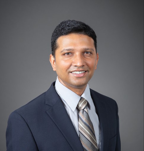
Chair: Dr. Anirban Bandyopadhyay, GlobalFoundries, USA
Learning Outcomes: In this tutorial, we’ll talk about the fundamentals of RF, mmWave and THz (>100GHz) radio covering different application and system requirements, circuits and design aspects and technologies. We’ll also highlight the key challenges to the radio system performance as we go to higher frequencies and how state-of-the -art technologies can address those challenges with innovations in materials, circuits, and system levels. The attendees will hear from some of the experts in this area how the future mmWave and Sub THz radio will look like and where current research is focused on at both industry and academic institutions for communication, sensing and spectroscopy.
Instructors:
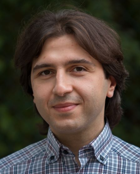
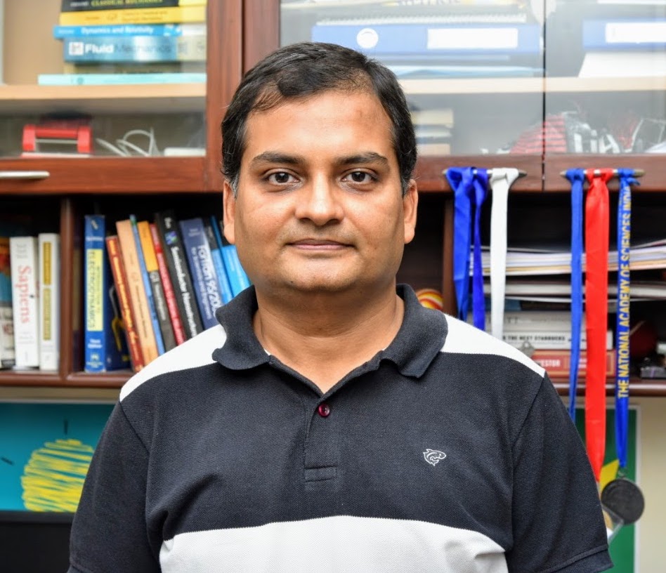
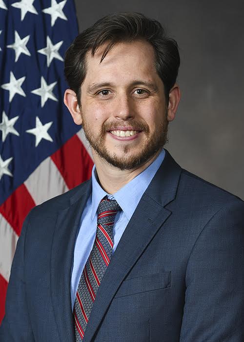
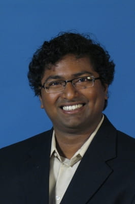
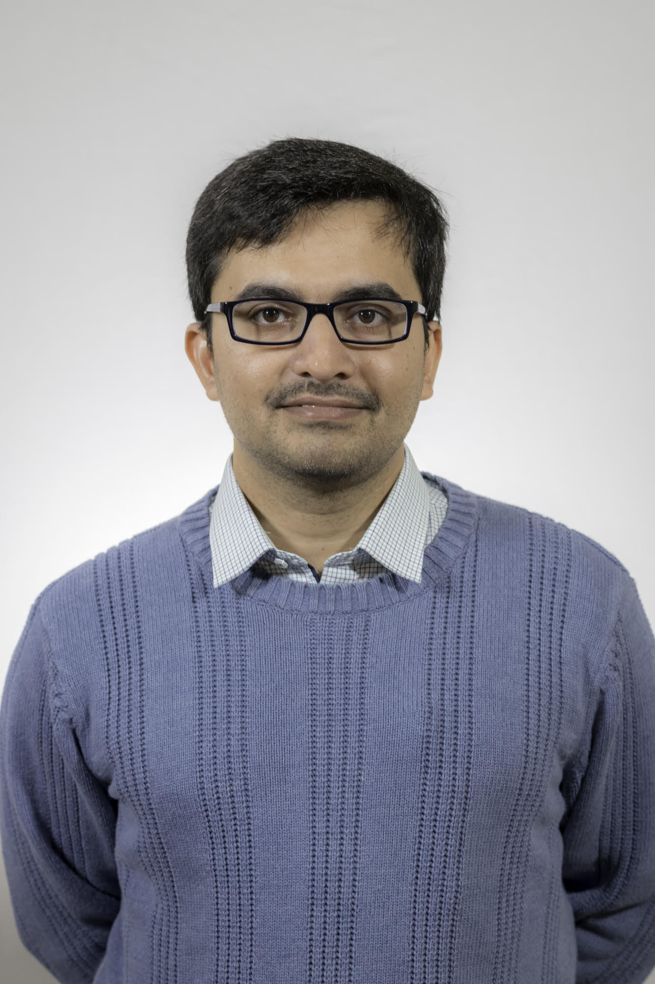
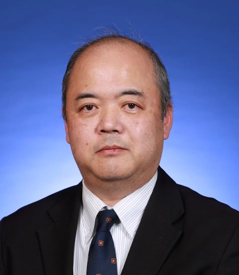
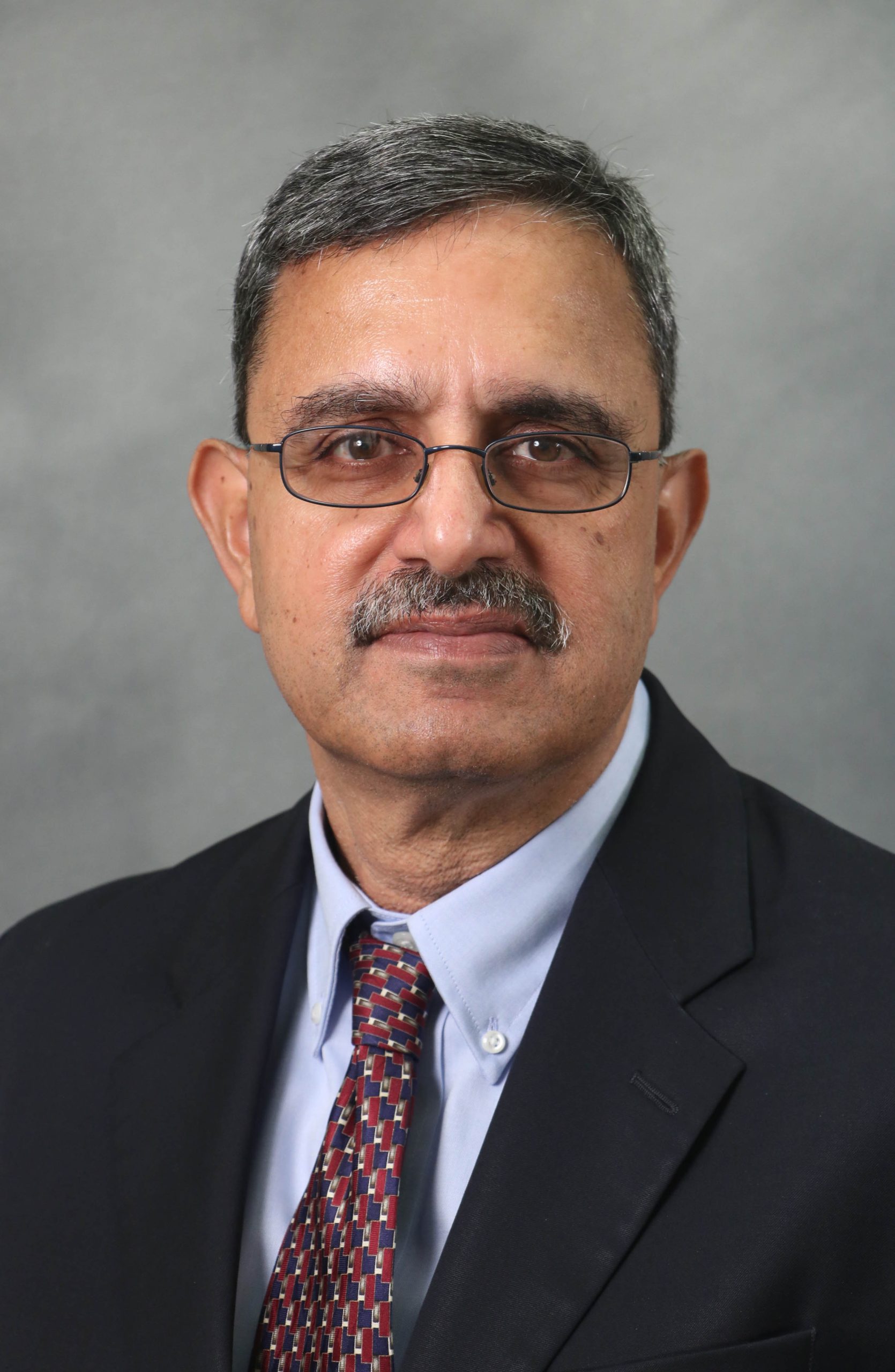
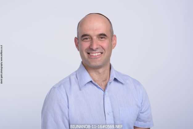
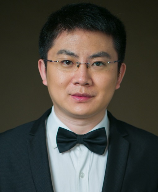
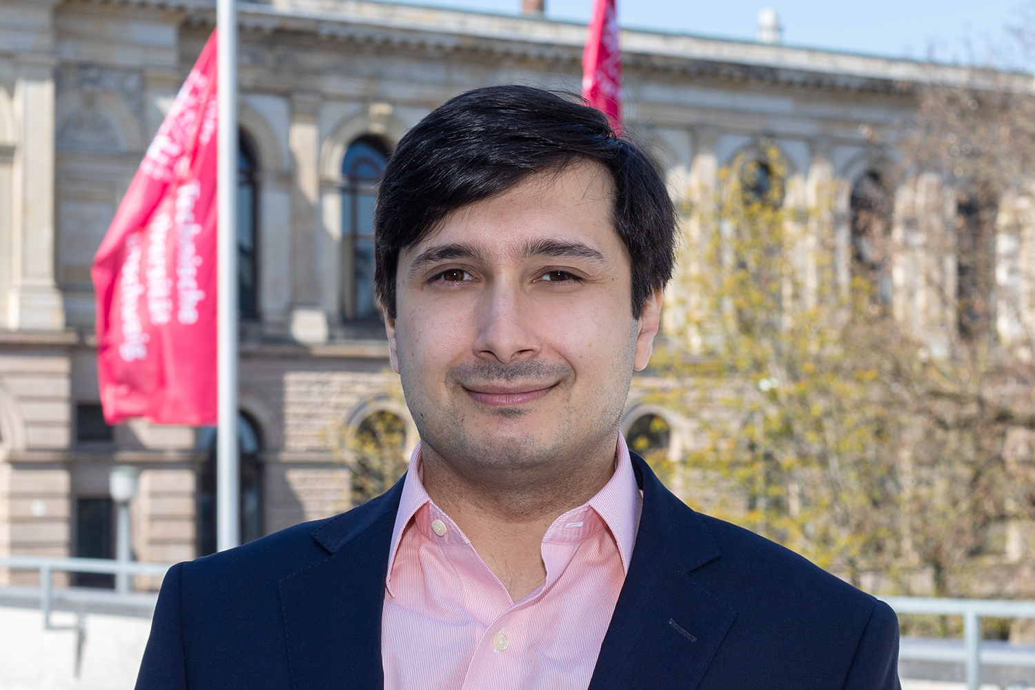
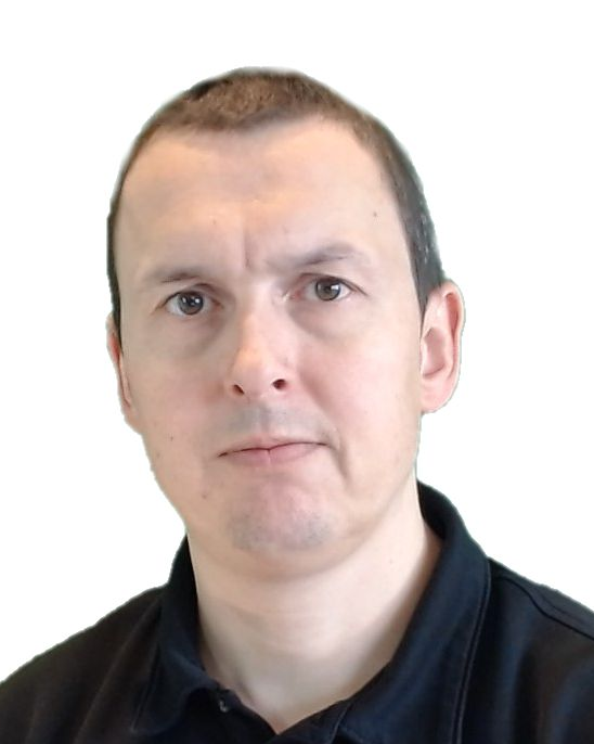
- Ned Cahoon, GF, USA
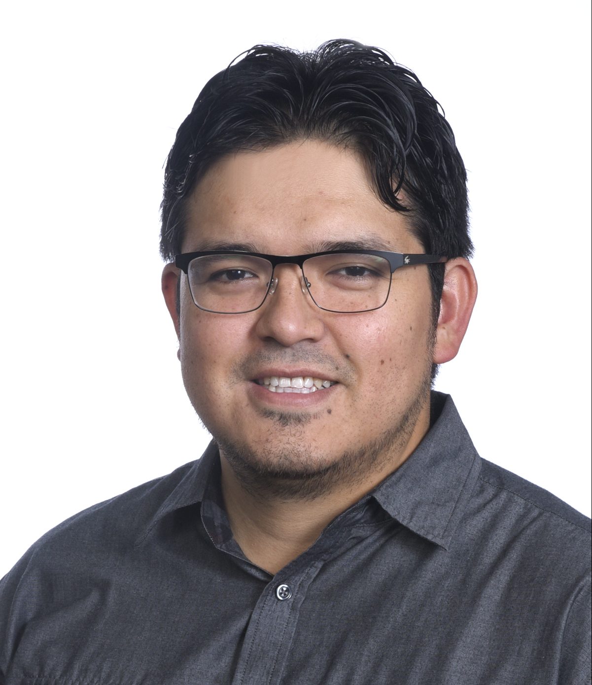
- Vadim Issakov, Universty of Braunschweig
- Venkata Vanukuru, GF
- Eric Desbonnets, SOITEC
- Dibakar Roychowdhury, Mahindra University
Key Topics covered
- Key challenges of a cellular radio link
- Why are higher frequencies like mmWave (24-100GHz) and sub-THz (>100GHz) needed
- Key challenges of mmWave and sub-THz Radio
- Different Phased array systems and beamforming techniques
Key learning goal:
Fundamentals of mm-wave Sub-THz radio, basics of phased array antenna and how it helps.
Key Topics covered
- Different Analog vs. RF vs. mm-Wave Design Approaches
- Fundamental Concepts of matching à to match or not to match
- Passive Components on-chip (TLine, Inductor, Transformer, Varactor)
- Design Basics and Challenges for Key blocks (LNA, PA, VCO)
Key learning goal:
Basic design methodologies for mm-wave and Sub-THz radio components
Key Topics covered
- Switch, LNA and PA integration on SOI/SiGe technologies
- Challenges and opportunities for RF and mmWave.
- Circuit innovations, technology features, KPI’s
- State of the art performance numbers for all the above circuit blocks.
Key learning goal:
Technology dependence of mm-Wave Switch, LNA PA performance, key challenges and innovative circuit techniques to address those.
Key topics covered:
- RF and mmWave Radio systems specifications for 5G advanced and future 6G requirements
- Comparison between bulk silicon, SOI, SiGe and non-silicon materials for 5G advanced and future 6G.
- Different THz sensing and spectroscopic techniques, pros and cons, trend
Key learning goal:
Comparison among different Si and non-Si technologies for mm Wave 5G and sub-THz 6G; how sensing works at THz frequencies, familiarity with different THz spectroscopic techniques and applications.
Tutorial – II: Industry Standard Compact Models for Advanced Semiconductor Devices
Chair: Prof. Yogesh Chauhan, IIT Kanpur, India
Learning Outcomes:
- Understanding of semiconductor device concepts
- Compact modelling techniques
- Implementation of compact model in circuit simulator
Instructors:
- Nihar Ranjan Mohapatra, IIT Gandhinagar, Gandhinagar
- Anjan Chakravorty, IIT Madras, Chennai
- Avirup Dasgupta, IIT Roorkee, Roorkee
- Somu Ghosh, Texas Instruments, Bengaluru
Key Topics Covered:
The compact model represents the behaviour of semiconductor devices in form of equations. The compact models play an important role in designing integrated circuits and serves as a bridge to share the information between foundries and circuit designers. Since various flavours of semiconductor devices have been proposed for a myriad of applications, the compact models have also evolved in last few decades. Accurate, fast, and robust compact models, which are capable of reproducing very complicated device characteristics are need of the hour.
Key learning goal:
Introduction to the compact model and art of compact modelling.
Key Topics Covered:
The MOS transistor architecture has evolved in last few decades. The semiconductor industry has progressed from bulk MOSFETs to FinFETs in 22nm CMOS technology and nanosheet FETs in 3nm CMOS technology. The device physics and device characteristics have also become complex.
This part of the tutorial will describe the BSIM family of industry-standard compact models for modern and future devices at advanced technology nodes. The discussion will range all the way from core models to the more involved second-order effects like quantum confinement, short-channel effects, noise etc.
Key learning goal:
Inner workings of the latest BSIM model framework and how it captures the characteristics of advanced devices efficiently.
Key Topics Covered:
The use of high-voltage and high-power MOS devices like Drain Extended MOS (DEMOS) transistors and Laterally Diffused MOS (LDMOS) transistors have been increasing since last two decades. The applications like automotive electronics, mobile communication, power conversion/conditioning in smart grids with renewable energy sources will not be possible without use of these devices. The device architecture, device characteristics and figures of merit of high voltage devices are completely different from the conventional MOS structures. The phenomena like on-state breakdown, off-state breakdown, quasi saturation, KIRK effect are unique to these devices.
Key learning goal:
HISIM-HV industry-standard compact model for silicon based high voltage devices. The discussion will range all the way from core model to the advanced models emulating different anomalous device behavior (like capacitance, internal drain voltage) of HV devices.
Key Topics Covered:
The Heterojunction Bipolar Transistor (HBT), an advanced version of Bipolar Junction Transistor (BJT), has been widely used in modern ultrafast circuits and in applications requiring high power efficiency (such as power amplifiers in communication systems). The HBTs have shown lots of promise for terahertz applications such as high-speed communications, spectroscopy and imaging. The bipolar devices are completely different from the MOS devices.This part of the tutorial will discuss the HICUM industry-standard compact models for HBTs. The discussion will start with a typical diode model implementation in Verilog-A followed by, (a) the introduction of the integral charge control relation (ICCR) based SPICE Gummel-Poon model for bipolar junction transistor and (b) modern heterojunction bipolar transistor model, HICUM.
Key learning goal:
1. 1-D intrinsic and 2-D internal HICUM model equivalent circuits, element formulations and corresponding parameter extraction strategies. 2. Recent improvements from perspectives of non-quasistatic delay, noise correlation and self-heating effects.
Key Topics Covered:
The compact models, after development, are included in the Process Design Kit (PDK). Along with the compact model, the PDK generally consists of files such as device library, design verification decks and design rule manual. The PDKs are released by the technology companies to the designers for circuit and system design with different technology nodes. In an enterprise environment, the designers consume and build on technology information using the PDK.
Key learning goal:
PDK development flow, consumables that go into the PDK and philosophy and design practices that are associated with building the PDK. This tutorial will provide an umbrella view of the PDK and unique aspects of building PDK for different CMOS technologies.
Tutorial – III: Neuromorphic Computing
Chair: Prof. Bipin Rajendran, King’s College London, UK
Learning Outcomes: To develop theoretical understanding on machine learning and neural networks. To understand requirements for its hardware implementation, and how to do digital, analog, and mixed-signal implementations of neuromorphic hardware.
Instructors:
- Chandramani Singh, IISc, Bangalore
- Debanjan Bhowmik, IIT Bombay
- Shubham Sahay, IIT Kanpur
- Sandip Mondal, IIT Bombay
Key Topics Covered:
The focus of this tutorial will be on the theoretical underpinnings of machine learning. We will start with a brief introduction of the machine leaning paradigms, i.e., supervised, unsupervised and reinforcement learnings. We will then have an overview of several learning techniques, e.g., linear regression, logistic regression, neural networks, backpropagation, K-means etc. We will touch upon the underlying mathematical tools like gradient descent, kernels, singular value decomposition etc. Finally, we will discuss complexities and performance measures of the above techniques and a few illustrative applications.
Key learning goal: Machine learning techniques
Key Topics Covered:
Neuromorphic computing will be introduced here both from a biology perspective and a computer-science/ machine-learning (ML) perspective. Importance of coming up with new hardware to implement the algorithms will be explained. As emerging hardware platforms, both analog/ mixed-signal hardware and digital hardware will be briefly introduced. Potential applications like edge artificial intelligence and robotics will also be covered.
Key learning goal: 1. Varied applications of Neuromorphic computing. 2. Hardware platforms for Neuromorphic computing
Key Topics Covered:
Digital and mixed-signal hardware for neuromorphic computing will be covered in details in this talk. Crossbar arrays of non-volatile memory (NVM) synaptic devices will be introduced in the context of mixed-signal hardware, with a discussion on how to perform multiply-accumulate (MAC) and Vector-by-Matrix Multiplication (VMM) operations on these arrays and the requirements from the synaptic devices for the purpose.
Key learning goal: Digital and mixed-signal hardware
Key Topics Covered:
The physics of operation of resistive random access memory (RRAM) devices will be covered here. It will be explained how such physics can be utilized to obtain biologically inspired synaptic behaviour in RRAM devices and make them suitable for analog and mixed-signal hardware applications, discussed in the previous talks.
Key learning goal: Physics of RRAM devices
Tutorial – IV: Biosensors and Flexible Electronics
Chairs: Prof. Siddhartha Panda, IIT Kanpur, India & Prof. Shree Prakash Tiwari, IIT Jodhpur, India
Learning Outcomes:
- Flexible bioelectronics on thread or textile substrate.
- To develop flexible bioelectronics for precision medicine using threads/textiles as substrate.
- Translation of biosensors towards products.
- Considerations for bringing a product into market
- Flexible Electronics: Challenges, Perspectives and Limitations for a rapidly expanding technology
Instructors:
- Sameer Sonkusale, Tufts University, USA
- Chandrasekhar Nair, Bigtec Labs, Bengaluru, India
- S. Sundar Kumar Iyer, IIT Kanpur, India
- Canterella Guiseppe, Free University of Bozen-Bolzano, Italy
Key Topics Covered:
This tutorial will explore the new realm of using threads and textile as an ultimate platform for flexible and stretchable bioelectronics. Threads offer unique advantages of universal availability, low cost, material diversity and simple textile-based processing. Interestingly, threads also provide an ideal platform for passive microfluidic sampling and delivery of analytes. In this talk, I will report reel-to-reel fabrication of functional smart threads for variety of sensing and electronics application. I will report on nanomaterial-infused smart threads for sensing strain and temperature. Nano-infused threads will be presented for sensing pH, glucose, lactate, ammonium and other chemical and biological biomarkers directly in biological fluids such as sweat or wound exudate. Beyond sensing and microfluidics, I will present recent progress on making super-thin transistors and electronics directly on thread and textile substrates. This new toolkit of highly flexible thread-based microfluidics, sensors, transistors and electronics makes it possible to realize wearable and implantable sensor platforms for health monitoring and treatment. The tutorial will showcase multiple applications for thread-based flexible biolectronics, such as wearable sweat sensing patches for monitoring metabolic health, smart bandages for treatment of chronic wounds, and smart sutures for detection and treatment of surgical infections. Tutorial will provide a roadmap for this emerging field and relevance to the ICEE scientific community.
Key learning goal: To develop flexible bioelectronics for precision medicine using threads/textiles as substrate.
Key Topics Covered:
This talk will cover the various challenges in translating a concept of a biosensor to a product in the market deployed at scale and the strategies to mitigate the risk of failure along the path of translation. The talk will draw heavily on the experiences in scaling Truenat as a Point of care platform for Infectious Disease Detection. The topics covered will include Target Product Profile definitions, market research and inputs, regulatory framework & guidelines (FDA/ CLSI/ WHO PQ), Initial research; from screening concepts to functional prototypes – criteria to be used, identification of critical technology element(s), Intellectual Property Rights: Defensive and Offensive ways, Product development eco-system – the gaps, TRL & MRL levels, FMEA and Technology transfer.
Key learning goal: Translation of biosensors towards products. Considerations for bringing a product into market.
Key Topics Covered:
The tutorial will start with an introduction and motivation for the emerging area of flexible electronics. The aspects this technology that makes it distinct from conventional electronics and its current limitations would be highlighted. The broad domains of active research and innovations in the area would then be discussed. The tutorial would conclude with some examples of successful and potential future implementation of the technology in real-world products and applications.
Key learning goal: An appreciation for the possibilities and limitations of the area of flexible electronics along with potential domains of research and innovation in that area.
Key Topics Covered:
This tutorial will guide the audience through a journey in the field of flexible electronics. Here, a broad plethora of sensors, circuits and systems, capable to withstand mechanical strain (i.e. bending, twisting, stretching, etc..), will be presented. First, an introduction and motivation will be given. Afterwards, the state-of-the-art will be presented, to provide a comprehensive overview in industrial and academic research. Next, materials, fabrication methods and devices will be presented, with a special focus on as stretchable, transparent and green electronics. Systems and real-application scenarios will be also explored. Finally, outlook and challenges for future market growth will be analysed.
Pre-Requisite: Basic knowledge of semiconductor physics and electronic devices.
Key learning goal: Comprehensive overview of a fast-growing technology, based on alternative fabrication strategies and materials.
Tutorial – V: Photovoltaics
Chair: Prof. Anil Kottantharayil, Professor, IIT Bombay, India
Learning Outcomes:
- Recent advances in organic materials for solar cells.
- Design rules and characterization for new materials for advanced devices. Advances in next-generation singlet-fission chromophores.
- Advanced characterization of commercial silicon solar cells.
- Photovoltaic Module Design and Reliability.
Instructors:
- Satish Patil, Indian Institute of Science, Bengaluru
- KL Narasimhan, Indian Institute of Science, Bengaluru
- Dinesh Kabra, Indian Institute of Technology Bombay, Mumbai
- Narendra Shiradkar, Indian Institute of Technology Bombay, Mumbai
Key Topics Covered:
The focus of this tutorial is novel materials. Primarily we shall discuss the class of organic materials used in most thin-film solar cell technologies. In organic photovoltaics, light absorption mostly happens in donor/acceptor heterojunctions. Recent advances in non-fullerene acceptors (NFA) have enabled more than 18% efficiency. Organic materials are also used as hole and electron transport layers. The performance of thin-film solar cells is often limited by the quality and stability of the perovskite/organic interface. Finally, organic chromophores undergo singlet-fission, which can increase the power conversion efficiency beyond the Shockley-Queisser limit. The tutorial will discuss the latest trends in NFAs, transport layers, and S-G chromophores. We shall explore the challenges and opportunities. We shall also discuss the essential characterization techniques.
Key learning goal: Design rules and characterization for new materials for advanced devices. Advances in next-generation singlet-fission chromophores.
Key Topics Covered:
The focus of this tutorial is the device physics of thin-film solar cells. Attendees will take a journey, from materials to devices, with solution-processable thin-film organic and perovskite photovoltaics. We will start with a primer on how to choose suitable materials. We shall discuss techniques to evaluate materials based on their photophysics. Specifically, we learn how to screen materials with advanced spectroscopic methods. Given the material properties, we shall learn how to fabricate and characterize thin-film photovoltaic devices. Finally, we shall appreciate the importance of material and device engineering to ensure that the lab-scale device can be upscaled and commercialized.
Key learning goal: How to select materials and design efficient devices for next-generation thin-film solar cells
Key Topics Covered:
This tutorial will focus on solar cell characterization with an emphasis on crystalline solar cells. The tutorial begins with a brief introduction to the basics of solar cells. This is followed by different methods to characterize solar cells- like quantum efficiency, photoluminescence imaging, implied Voc, PFF etc. The tutorial will conclude with a brief discussion of the limitations of the Al-BSF architecture and how advanced architectures like PERC, TOPCON and HJT improve performance.
Key learning goal: Defect analysis and troubleshooting of silicon solar cells.
Key Topics Covered:
Eventual goal of any solar cell technology is to deliver desired performance for several decades in often harsh end-use environments. This is a crucial factor in the commercial success of any PV technology. In this tutorial, we will discuss the design of Photovoltaic modules, materials, and components. We will also look at key performance metrics for PV modules and reliability issues found in the field. Eventually, we will discuss the ways to design high-quality, reliable PV modules.
Key learning goal: Designing of reliable Photovoltaic modules and their performance metrics
